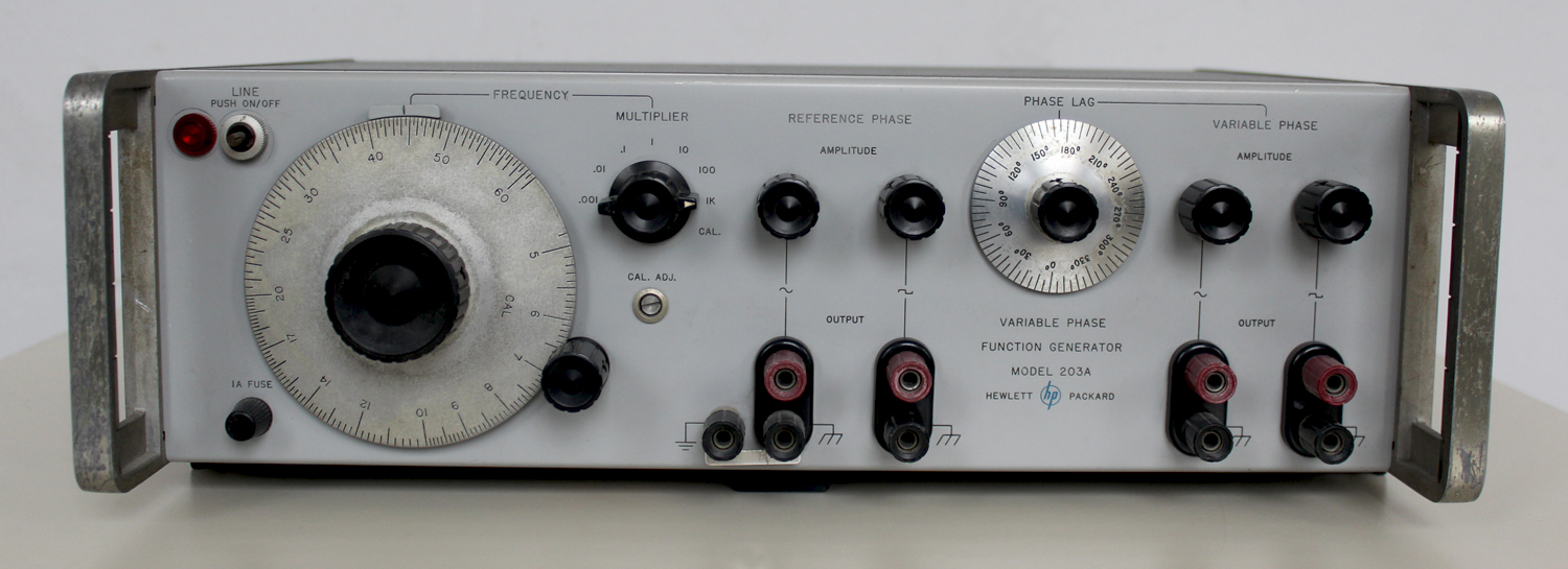
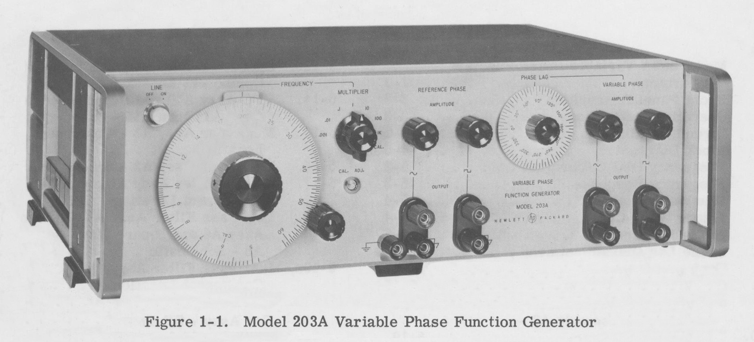
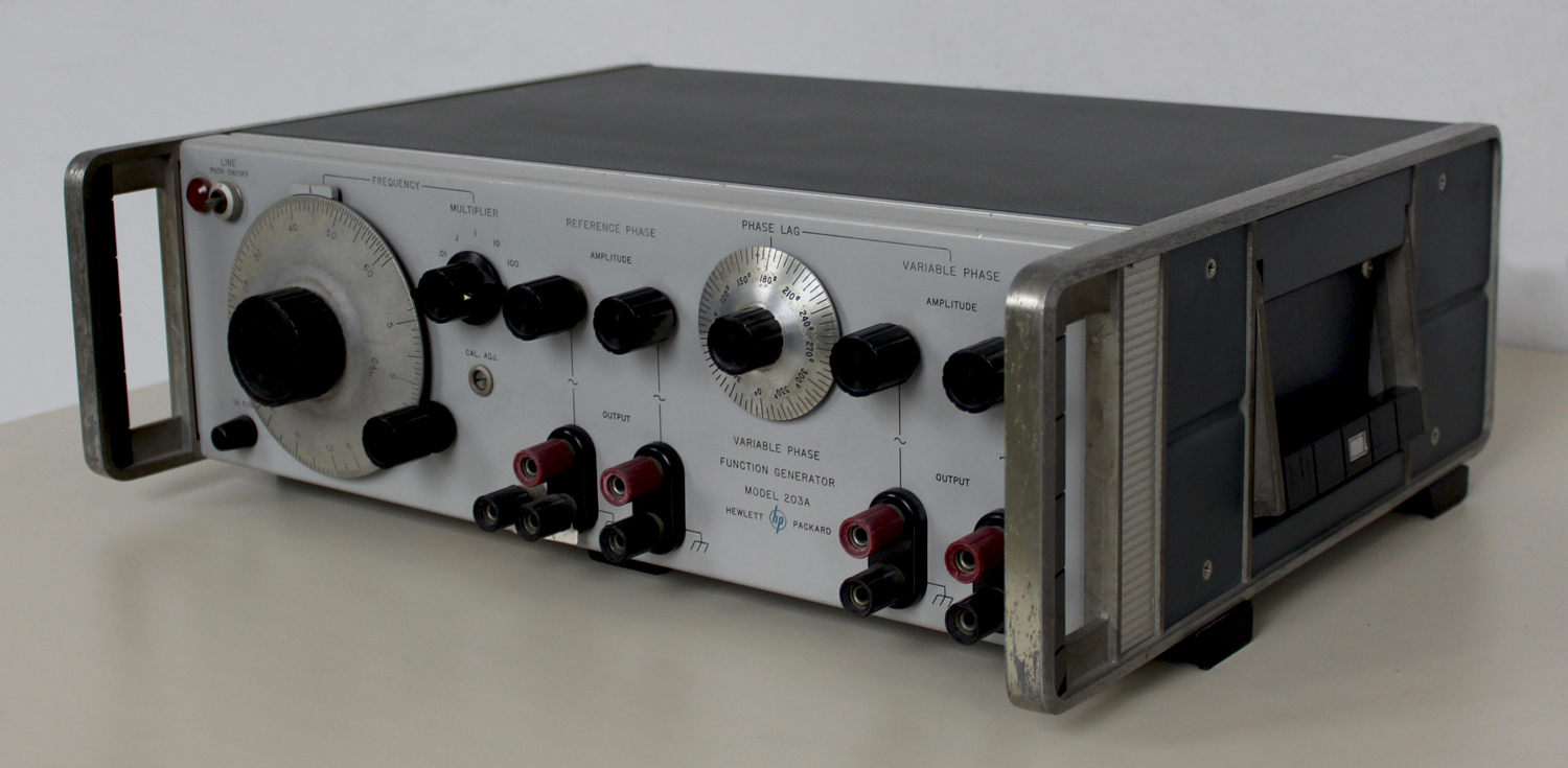
 Variable Phase Function Generator, Model 203A, Yokogawa Hewlett Packard. Seconda parte.
Per cause indipendenti dalla nostra volontà non disponiamo dell’inventario generale dell’epoca.
Nell’inventario per reparto N° 7 di Elettronica, in data febbraio 1968, al n° D 4224 si legge: “Function Generator 203/A”.
Ma ce ne sono due esemplari: questo è stato costruito dalla Yokogawa Electric alleata della Hewlett Packard, Tokyo.
In rete si trovano vari documenti, manuali di istruzioni e altre informazioni ai seguenti indirizzi:
http://hparchive.com/Manuals/HP-203A-Manual-sn425.pdf
http://www.hpl.hp.com/hpjournal/pdfs/IssuePDFs/1965-07.pdf
Presso la Sezione Elettronica è conservato il manuale di istruzioni nel quale si trovano note e disegni aggiunti a matita delle riparazioni fatte negli anni. Noi le abbiamo tolte per ridare ai disegni l’aspetto originale.
Il testo delle istruzioni prosegue dalla prima parte.
§§§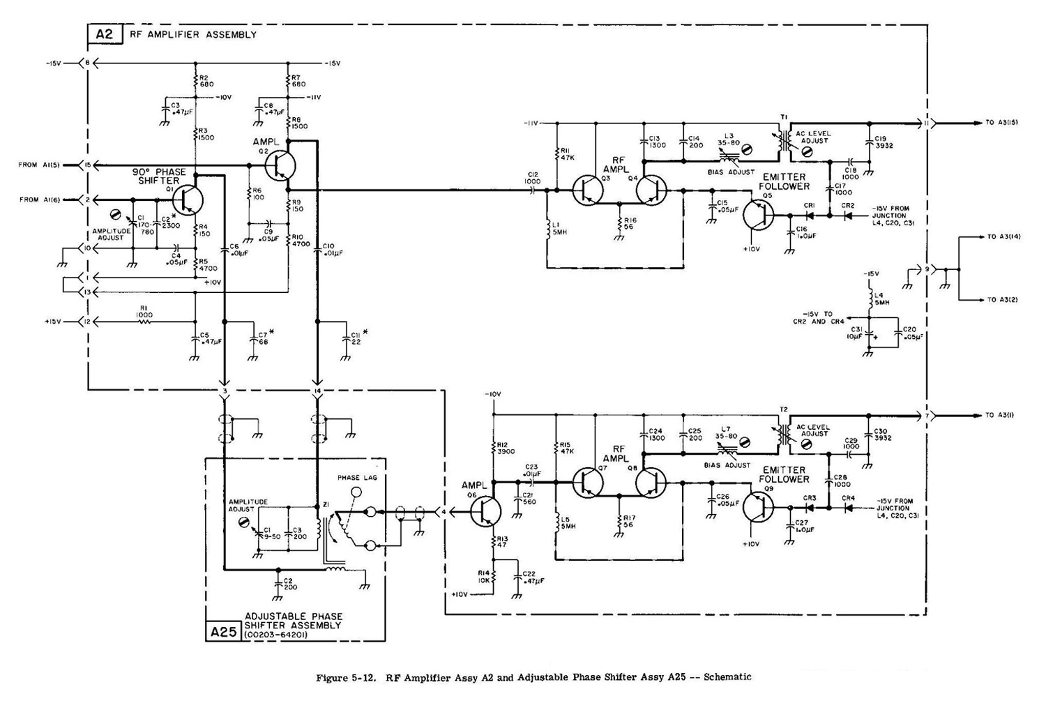
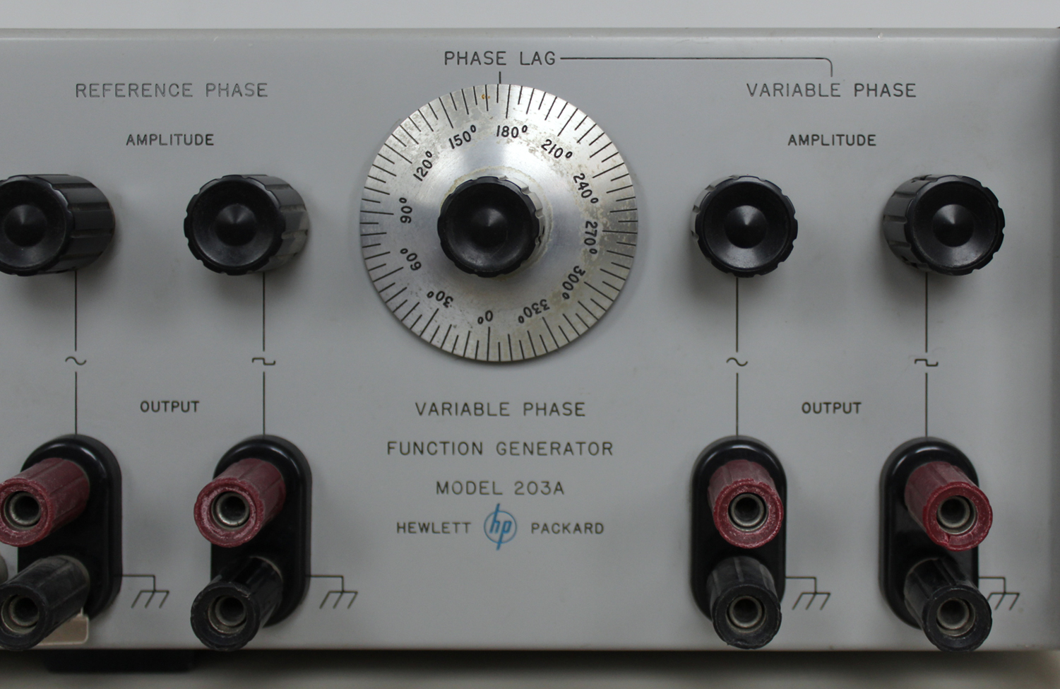
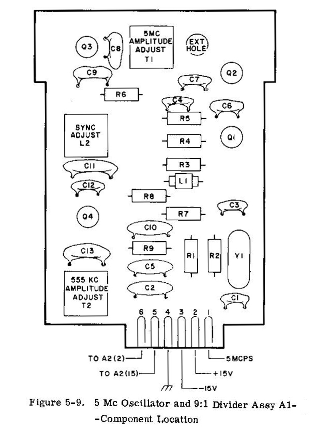
«4-16. VARIABLE PHASE SHIFTER ASSEMBLY.
4-17. The variable phase shifter assembly A25 (figure 5-12) is a goniometer consisting of two stator windings, a rotor winding, and associated circuits. The goniometer requires two 555 kc input signals; one from A2Q2 to one of the stator windings, and the other from A2Q1 and the 90° phase shift network to the other stator winding. The output phase corresponds to the angle of the rotor winding (PHASE LAG control). The phase can be continuously adjusted from 0° through 360° with respect to the reference signal while maintaining a constant amplitude. The adjustable phase shifter output is applied to the RF amplifier assembly A2 (figure 5-12).
4-18. RF AMPLIFIERS (A2].
4-19. The RF amplifier assembly A2 consists of two RF amplifiers; A2Q3, A2Q4, and A2Q5 for the reference phase channel and A2Q6 through A2Q9 for the variable phase channel. Refer to the schematic diagram (figure 5-12) for circuit details.
4-20. VARIABLE PHASE CHANNEL RF AMPLIFIER.
4-21. The signal from the variable phase shifter is amplified by A2Q6,then applied to the base of A2Q7. A2Q7 and A2Q8 act as an over-driven amplifier which amplifies and clips the signal applied to the base of A2Q7; this operation produces a square wave of current at the collector of A2Q8. The zero crossing of the square wave of current coincides with the zero crossing of the sine wave signal applied to the base of A2Q7 so that the phase of the applied signal is preserved. A tuned network, formed by A2C24, A2C25, A2C29. A2C30, A2L7, and A2T2 filters the 555 kc square-current waveform to a nearly pure sine wave.
4-22. The output of the RF amplifier circuit, which is taken across A2C30, is maintained at a constant amplitude by the level controlling circuit. If the output should increase, the voltage at A2C27 increases, resulting in a voltage increase at the base of A2Q9. This increase is applied to the bases of A2Q7 and A2Q8 which then conduct less average current. When A2Q8 conducts less the signal at its collector decreases and the output voltage decreases, opposing the original change. The result is that the amplitude of the output remains nearly constant despite variations in the amplitude of the input signal. The output signal is then applied to ABT4 in the modulator assembly A3 (figure 5-16).
4-23. REFERENCE PHASE CHANNEL RF AMPLIFIER.
4-24. The signal present at the emitter of A2Q2 is applied to the reference phase channel RF amplifier section, A2Q3 through A2Q5. This stage operates the same as the variable phase channel RF amplifier described in paragraph 4-20. The output signal is then applied to A3T3 in the modulator assembly A3.
4-25. VARIABLE FREQUENCY OSCILLATOR (A10)
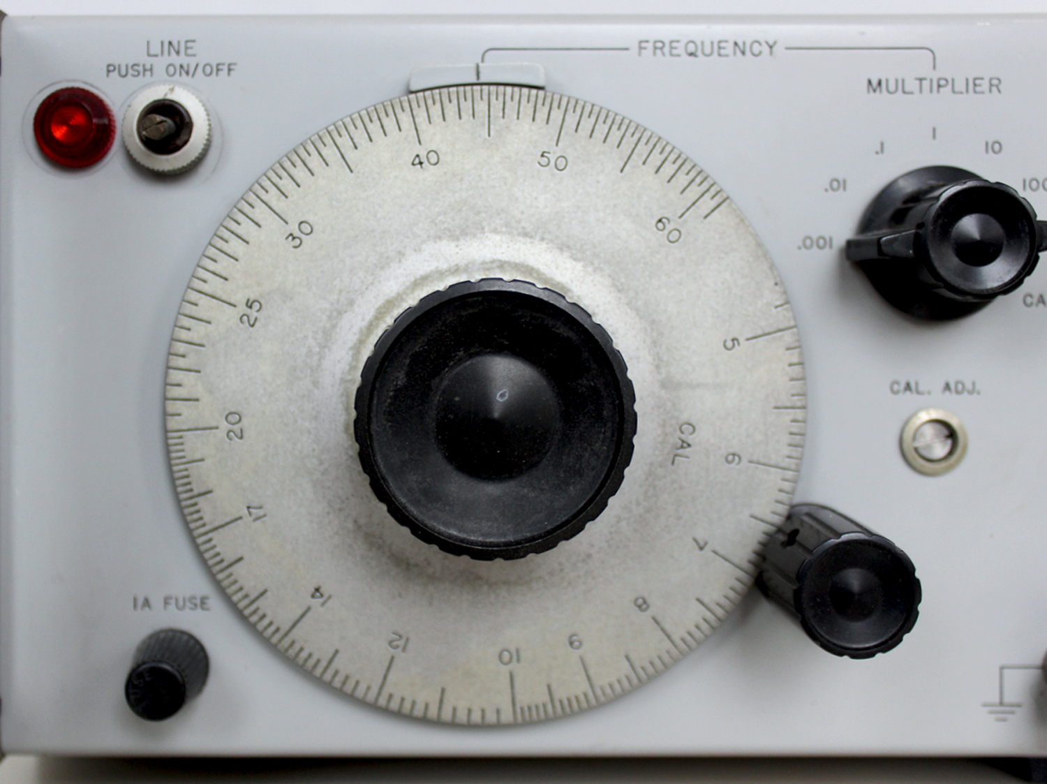
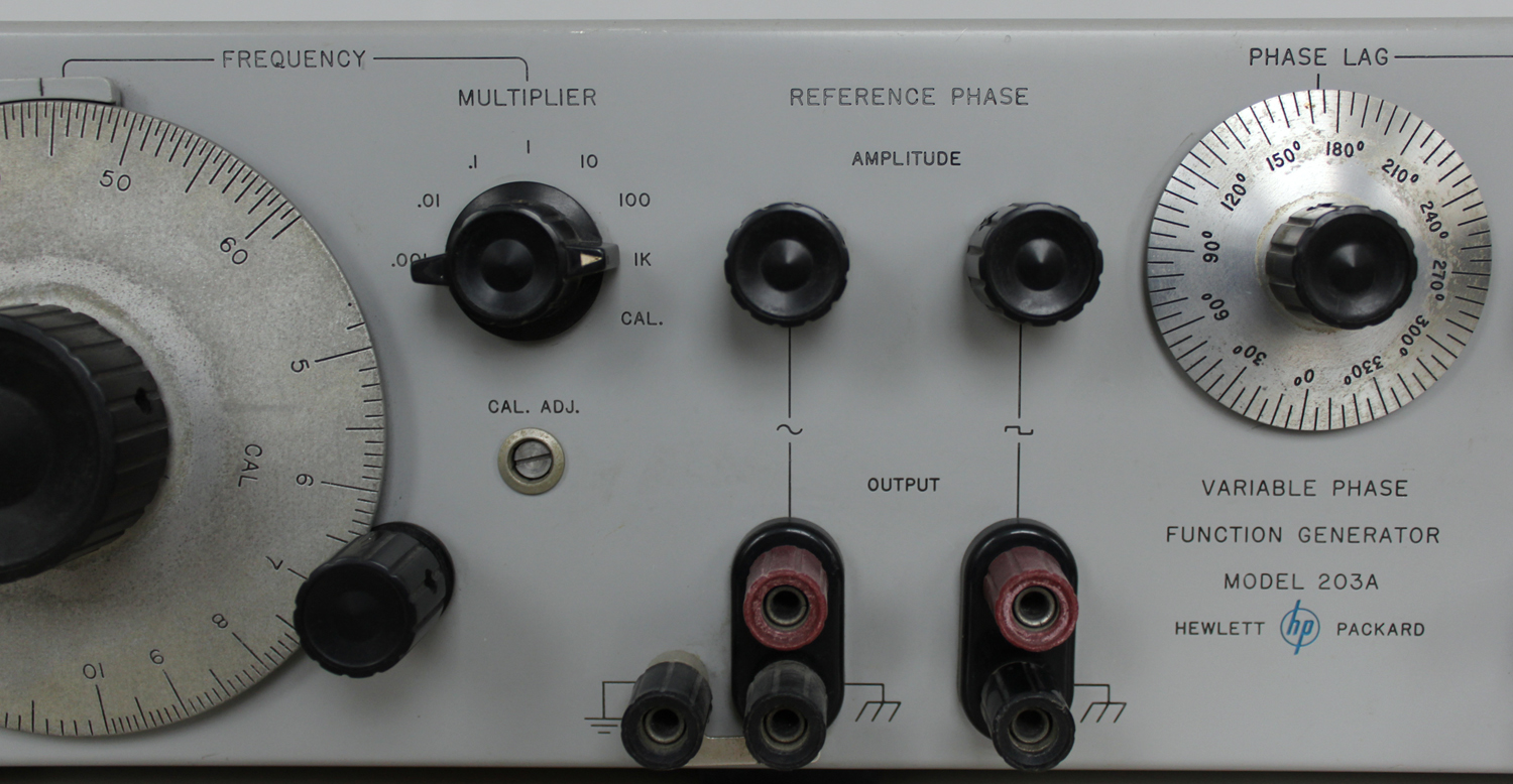
4-26. The variable frequency oscillator assembly A10 generates a signal that is variable from 495 kc to 550 kc by rotation of the front panel FREQUENCY dial. The FREQUENCY dial is calibrated so that with the dial set at 5 the VFO is oscillating at 550 kc and with the dial set at 60 the VFO is oscillating at 495 kc. The output signal from the variable frequency oscillator is applied to the 1 K position of the MULTIPLIER (frequency range) switch and also to the 1st decade module. Refer to the schematic diagram, figure 5-14, for circuit details.
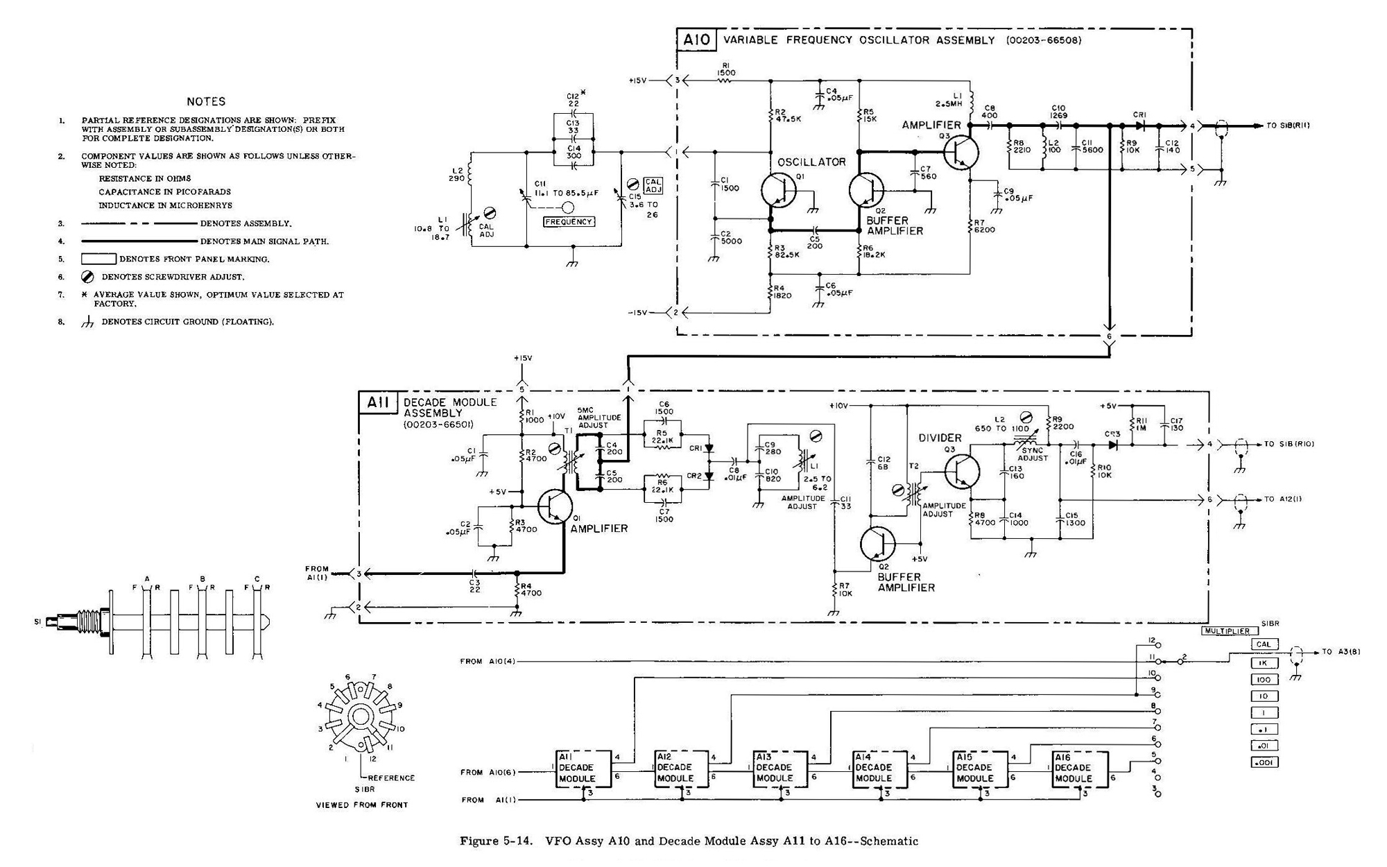
4-27. DECADE MODULES (A11-A16).
4-28. The six decade module assemblies A11 thru A16 each consist of a mixer, a bandpass filter, and a 10:1 divider. These decades produce a band of high frequency signals that are mixed in the modulators (A3) with the 555 kc fixed frequency signal from the RF amplifiers to produce a signal in the 0.005 cps to 60 kc range (refer to paragraph 1-5 for options]. Refer to the schematic diagram, figure 5-14 and figure 4-1 for circuit details.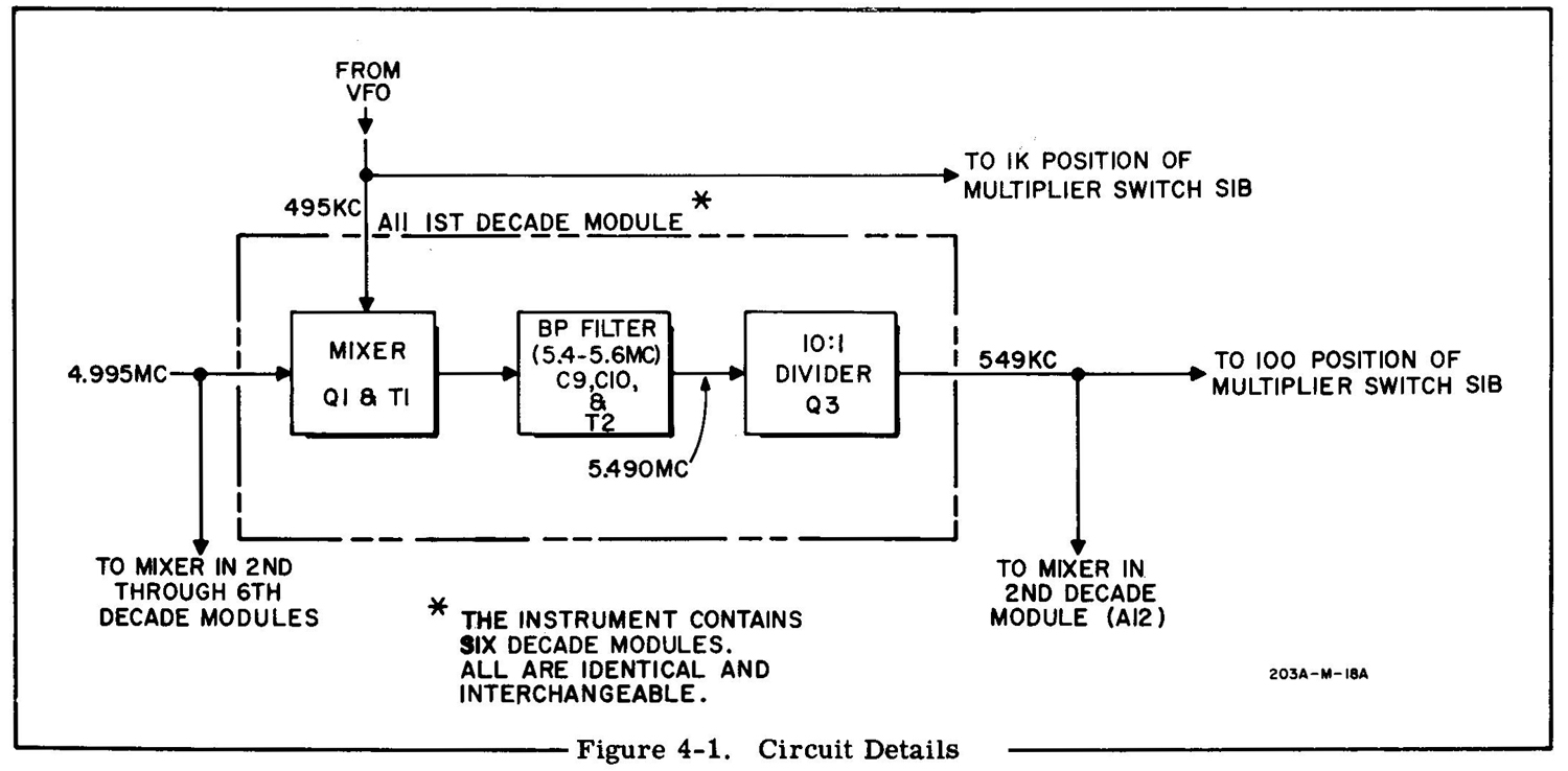
4-29. DECADE MODULE (A11). 4-30. The 4. 995 Me signal from the crystal oscillator is applied to the emitter of A11Q1 isolation stage, and subsequently appears across the primary of A11T1. The signal from A11T1 is applied to a suppressed carrier, balanced modulator. The 495 kc VFO signal (assume that the FREQUENCY dial is at 60 and the VFO signal is 495 kc) is applied to the other input of the balanced modulator. Both signals are mixed, and the sum and difference of these two frequencies will appear at the output. The signal from the balanced modulator is passed through an LC filter network which is tuned for a band-pass of from 5. 4 Me to 5. 6 Mc, which only allows the sum frequency to pass on to the 10:1 divider A11Q3. The 10:1 divider is similar to the 9:1 divider described in paragraph 4- 9; the main difference being that the tuned tank circuit in the 10:1 divider is adjusted so that the stage provides an exact 10:1 division of the input frequency. The resultant frequency is fed to the 100 position of the FREQUENCY MULTIPLIER switch and to the mixer in the second decade module A12.
4-31. DECADE MODULES, A12 THROUGH A16.
4-32. The action within the succeeding decade modules is the same as that described for the first decade module A11. The output of each module is applied to a position of the FREQUENCY MULTIPLIER switch and to the mixer in the following decade module. Thus a set of variable frequency signals are produced and when mixed with the
constant high-frequency signal in the modulator (A3) a beat frequency is produced. The beat frequency is decreased by a factor of 10 for each lower range of the FREQUENCY MULTIPLIER switch.
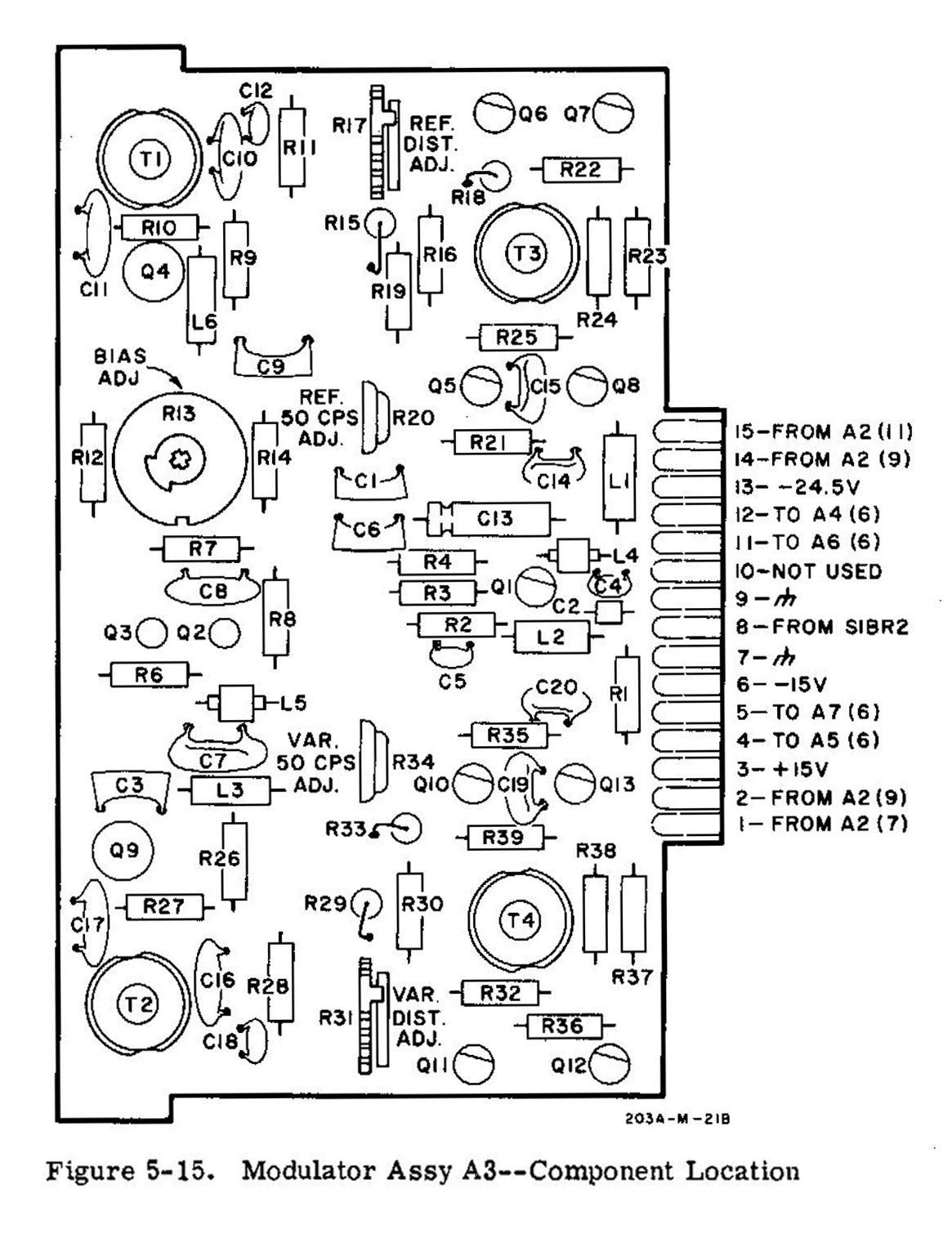
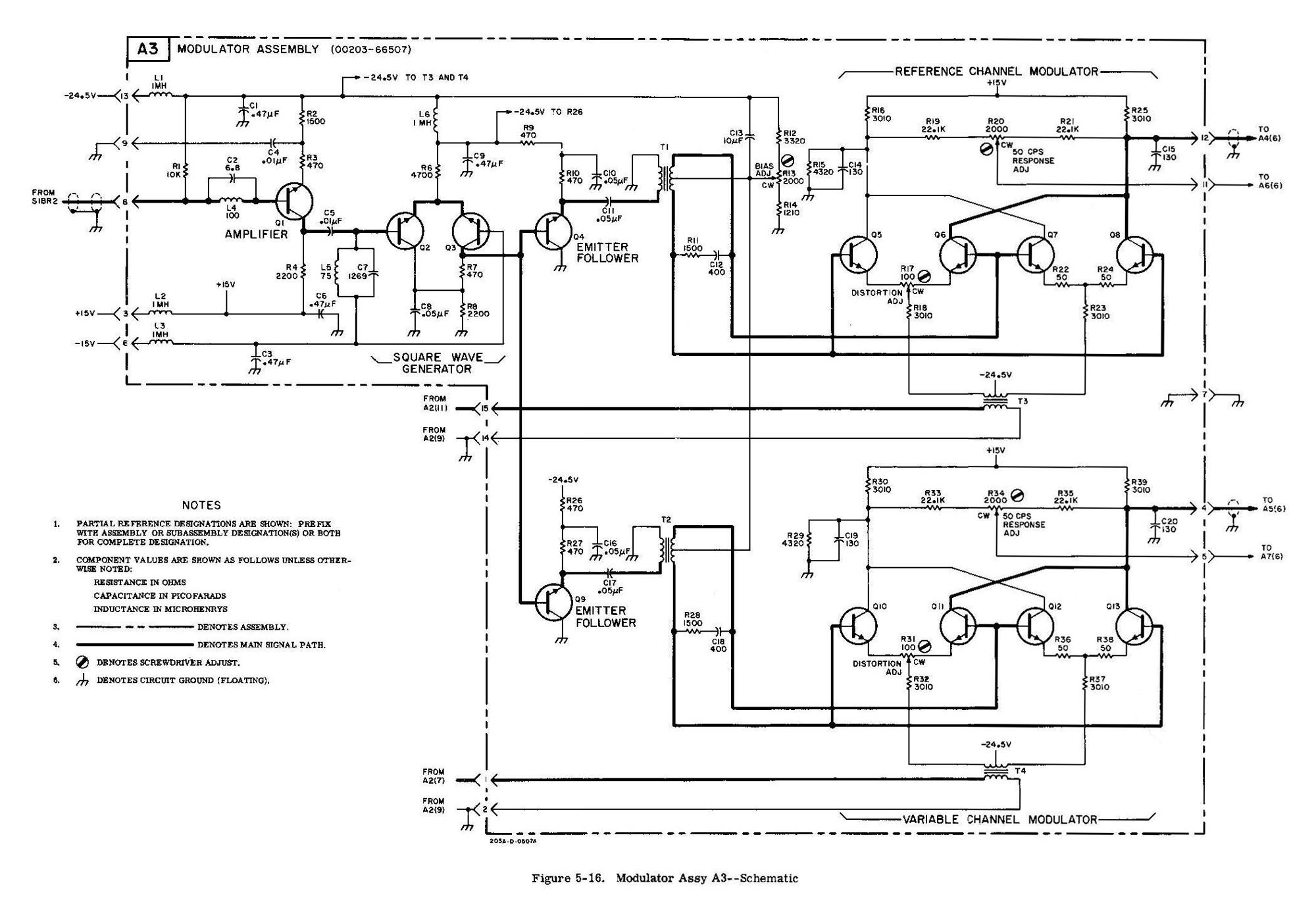
4-33. MODULATOR ASSEMBLY, A3.
4-34. The Modulator assembly A3 consists of a modulator drive amplifier and two balanced switching type modulators; one for the REFERENCE PHASE channel, and the other for the VARIABLE PHASE channel. Refer to the schematic diagram, figure 5-16, for details.
4-35. MODULATOR DRIVER AMPLIFIER.
4-36. The frequency selected by the FREQUENCY dial and the FREQUENCY MULTIPLIER is applied to the input of the modulator driver amplifier A3Q1 where it is amplified and applied to A3Q2 and A3Q3. A3Q2 and A3Q3 act as an over driven amplifier which amplifies and clips the signal applied to the base of A3Q2. This operation produces a square wave output at the collector of A3Q3 which is applied to the modulator section as a switching signal.
4-37. REFERENCE PHASE CHANNEL MODULATOR.
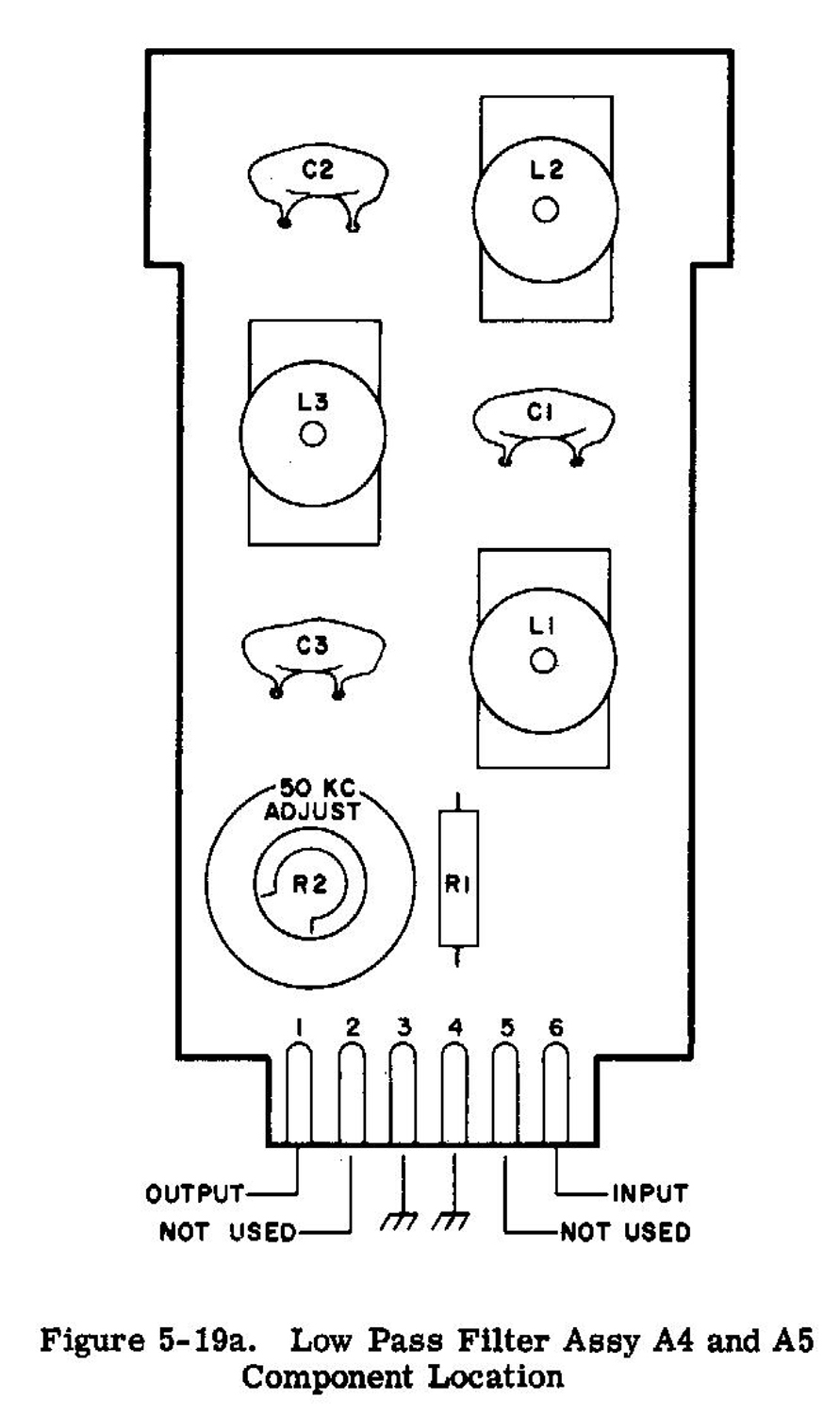
4-38. The modulator driving signal (VFO) and decade output is applied to the bases of the switching transistors (A3Q5 thru A3Q8). The fixed frequency, a 555 kc sine wave, is applied through series resistors to the emitters of the switching transistors. The output at the collectors is sine wave of the sum and difference frequencies. This signal is applied to the low pass filter assembly A4 (figure 5-18), The filter passes only the difference frequency, the output is a sine wave having a frequency that is between 0.005 cps and 60 kc depending on the position of the FREQUENCY MULTIPLIER switch and the FREQUENCY dial setting (refer to paragraph 1-5 for Options). The output signal is applied to the dc amplifier A6.
4-39. A dc reference voltage is derived by summing the signals at the collectors of A3Q5 and A3Q6. This dc reference voltage is used as a reference voltage for the differential amplifier in the dc amplifier assembly A6.
4-40. VARIABLE PHASE CHANNEL MODULATOR.
4-41. The variable phase channel modulator operates the same as the reference phase channel described in paragraph 4-37, except that the output is applied to the Low Pass Filter A5 and then to the dc amplifier A7.
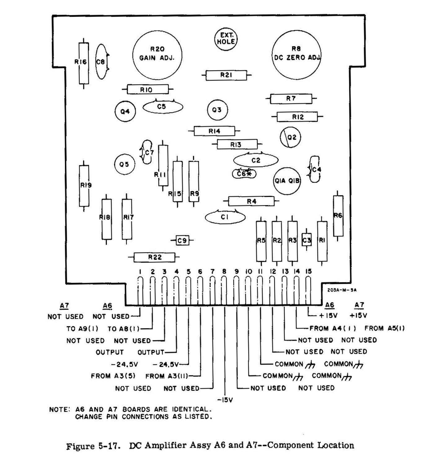
4-42. DC AMPLIFIER ASSEMBLIES A6 AND A7.
4-43. After passing through the low pass filter the signal is fed to the direct coupled amplifiers; A6 for the reference phase channel, and A7 for the variable phase channel. Refer to the schematic diagrams figures 5-18 and 5-20 for circuit details.
4-44. REFERENCES PHASE CHANNEL DC AMPLIFIER ASSEMBLY.
4-45. The dc amplifier uses a differential amplifier for the input stage. The dc reference voltage from the modulator section is used as the reference input for the differential amplifier. This configuration minimizes any tendency of dc drift due to power supply temperature variations. The dc amplifier circuit uses negative feedback to provide for low distortion amplification. The output is applied to a bridged-T type attenuator and the square wave generator A8. 4-46. VARIABLE PHASE CHANNEL DC AMPLIFIER ASSEMBLY. 4-47. The variable phase channel dc amplifier operates the same as the reference phase channel described in paragraph 4-44, except that the output is applied to bridged-T type attenuator and the square wave generator, A9.
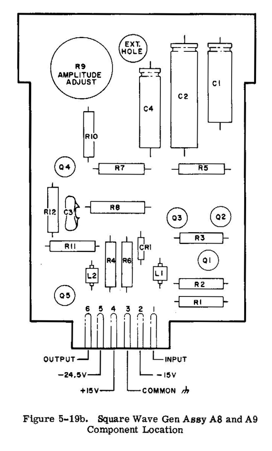
4-48. SQUARE WAVE AMPLIHER ASSEMBLIES A8 AND A9.
4-49. The output sine wave from the dc amplifier is applied to a square wave generator section, AB, for the REFERENCE PHASE channel, and A9 for the VARIABLE PHASE channel. Refer to the schematic diagrams, figures 5-18 and 5-20, for circuit details.
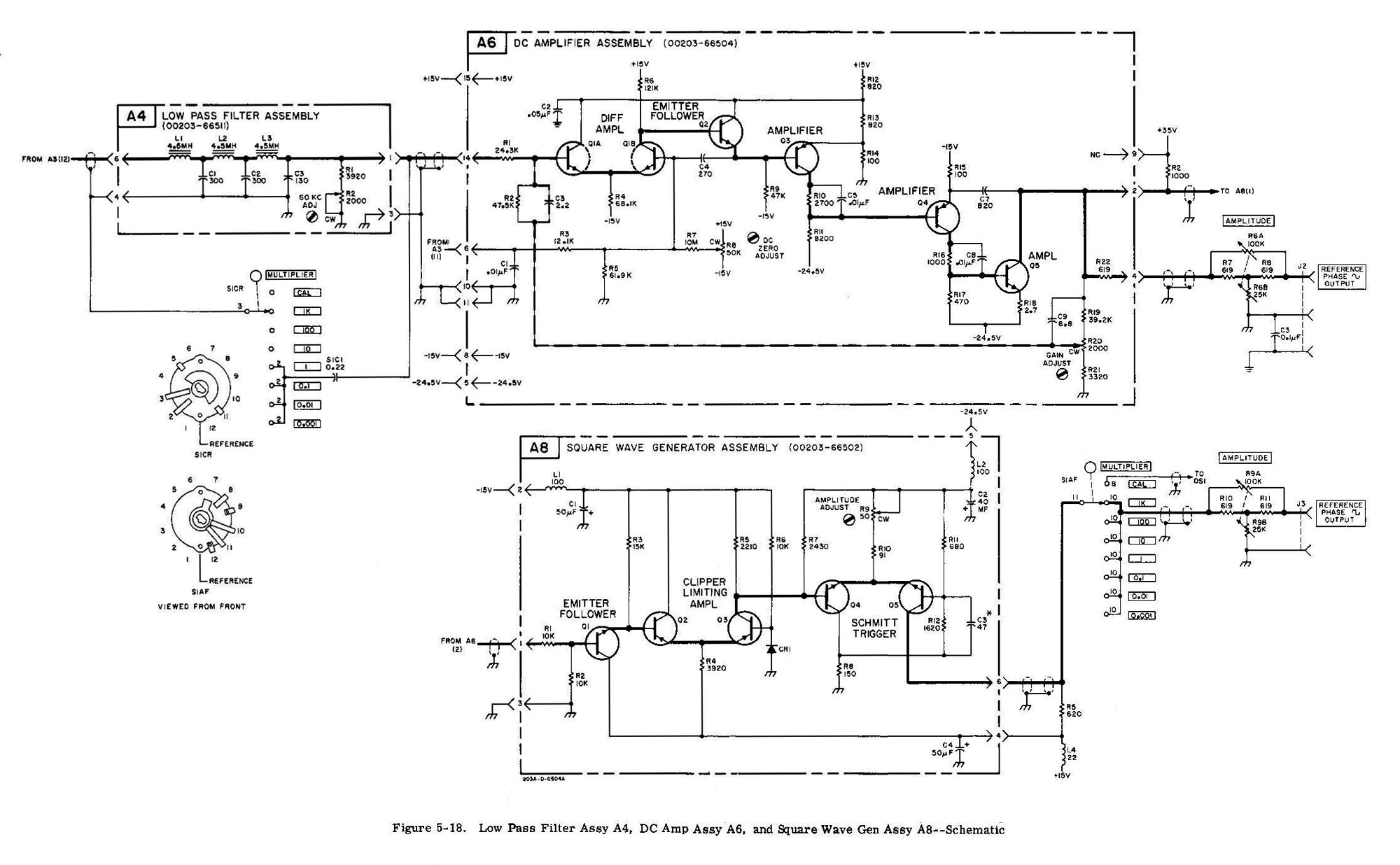
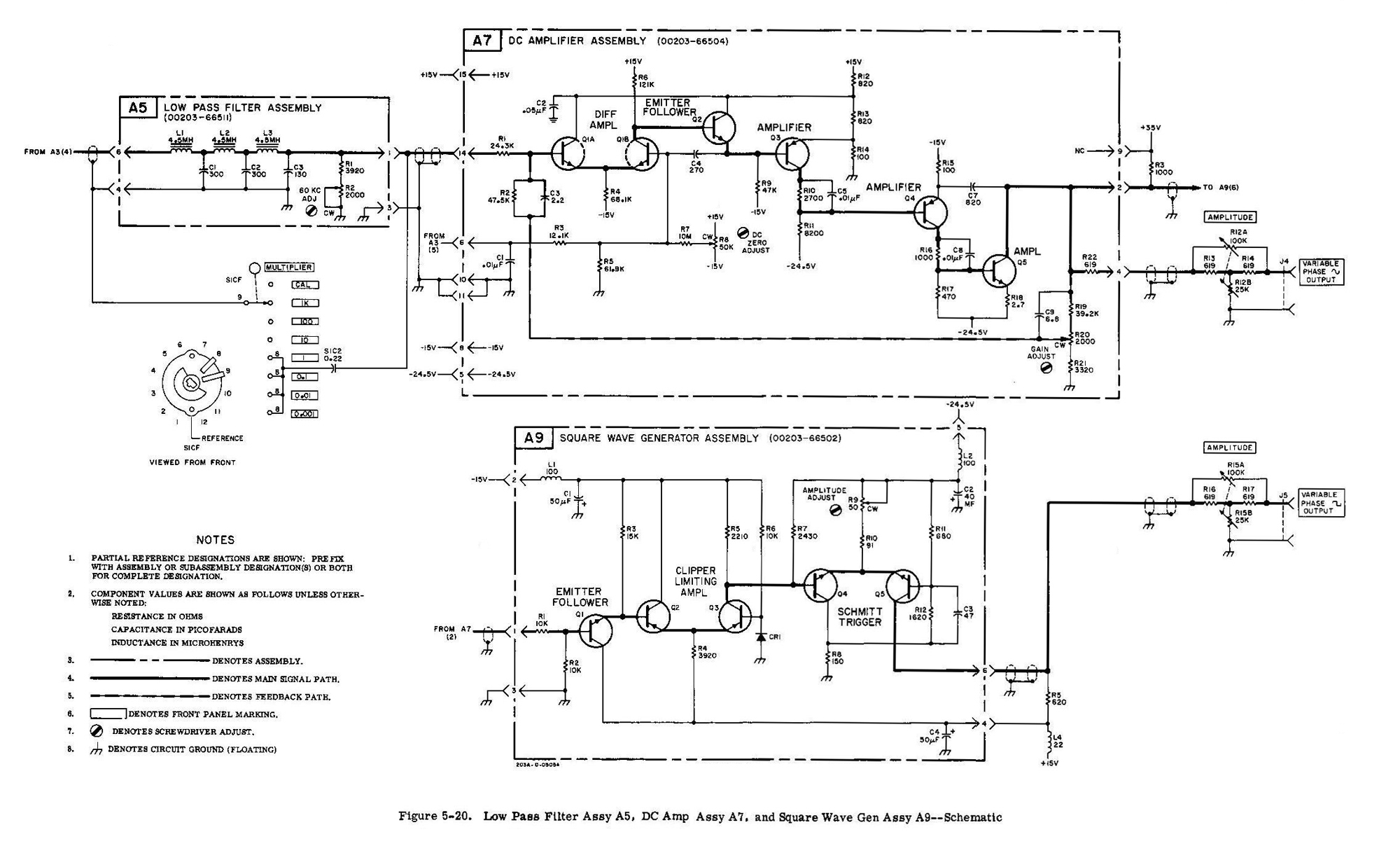
4-50. REFERENCE PHASE CHANNEL SQUARE WAVE GENERATOR.
4-51. The sine wave from the dc amplifier is amplified by A8Q1 then applied to the base of A8Q2. A8Q2 and A8Q3 act as an over driven amplifier which amplifies and clips the signal applied to the base of A8Q2, and produces a square wave at the collector of A8Q3. This square wave is applied to A8Q4 and A8Q5 which form a Schmitt trigger circuit. The Schmitt trigger is a regenerative circuit which changes states abruptly when the input signal crosses a specific dc triggering level. The output from this stage is a square wave having a rise time of less than 0.2 microsecond with the same frequency and phase as the sine wave signal applied to the circuit. The output is applied to a bridged-T attenuator.
4-52. VARIABLE PHASE CHANNEL SQUARE WAVE GENERATOR.
4-53. The variable phase channel square wave generator operates the same as the reference phase channel described in paragraph 4-50.
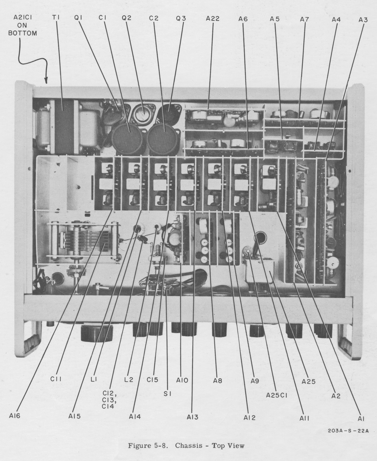
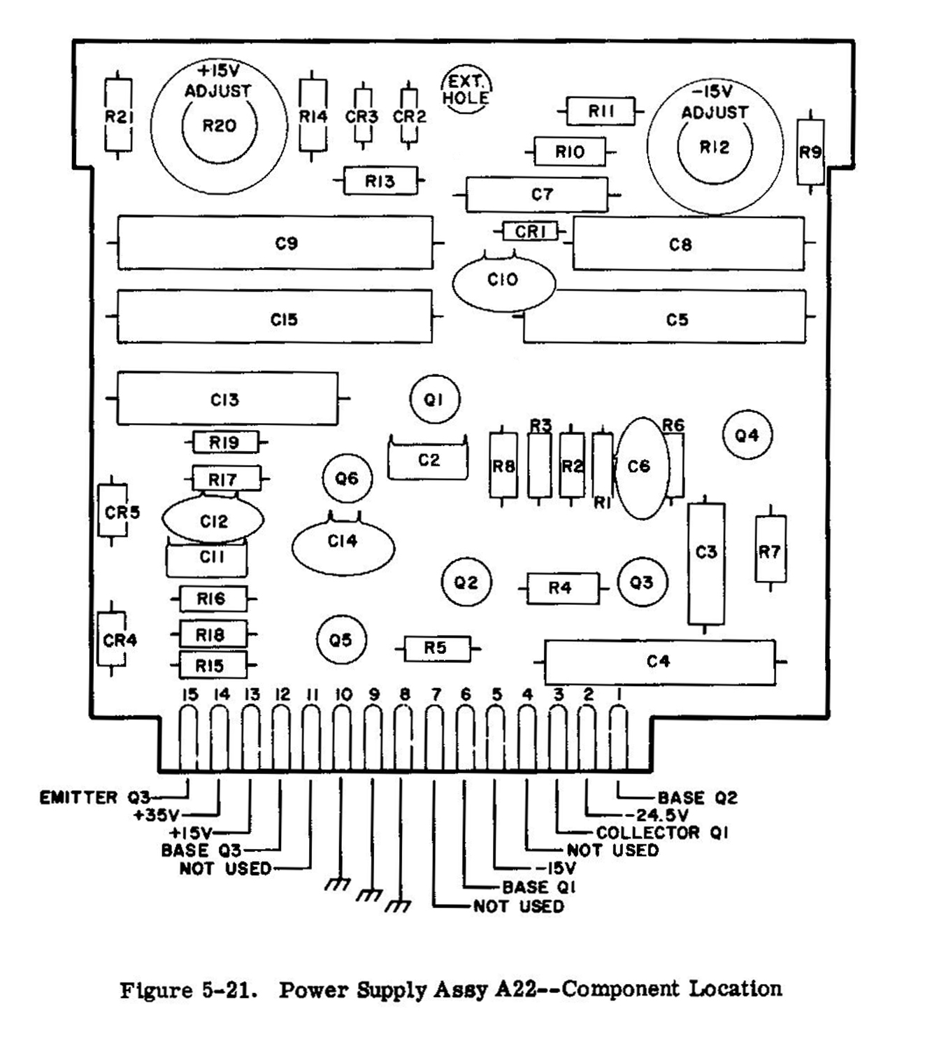
4-54. DC POWER SUPPLY A21. A22.
4-55. The dc power supply provides regulated +15, -15, and -24.5 volts and unregulated +35 volts.
4-56. CALIBRATION FEATURE.
4-57. A quick check for calibration of the frequency dial is a comparison between instrument and line frequency. The FREQUENCY dial is set to 6 (CAL) and the FREQUENCY MULTIPLIER is set to the CAL position. Through S1BR a 60 cycle output from A11 is applied to the pilot light which will mix with the 60 cycle line frequency. The pilot light will flicker at the difference or beat rate. This rate may be adjusted to minimum by the CAL ADJ control which slightly affects the VFO frequency. At a minimum rate of flicker the instrument’s 60 cycle frequency will be most nearly like the 60 cycle line frequency. For checking the exact frequencies throughout the ranges see paragraph 5-5 Frequency Dial Calibration».
§§§
Per consultare la prima parte scrivere “203A” su Cerca.
Foto di Claudio Profumieri, elaborazioni e ricerche di Fabio Panfili.
Per ingrandire le immagini cliccare su di esse col tasto destro del mouse e scegliere tra le opzioni.