
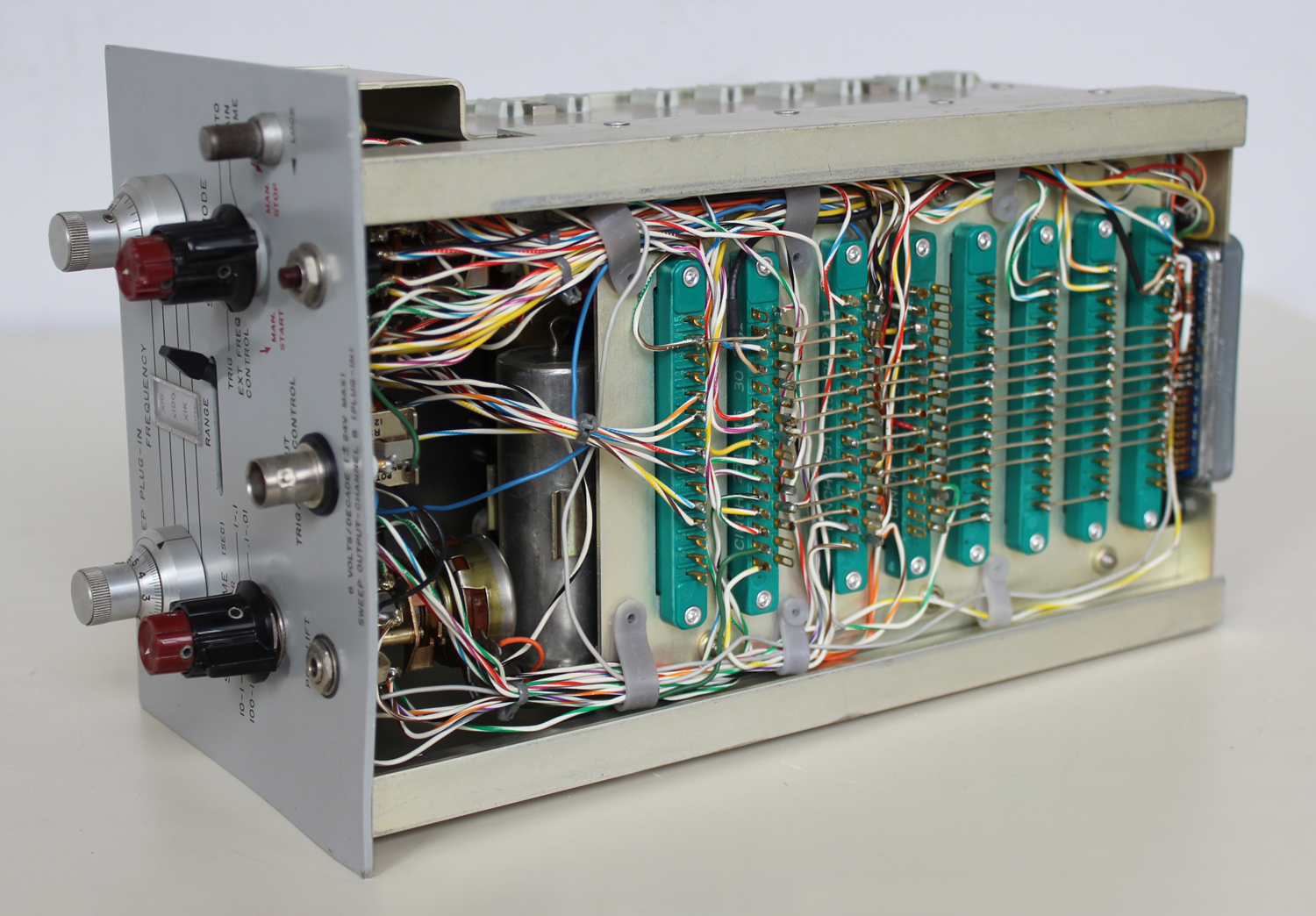
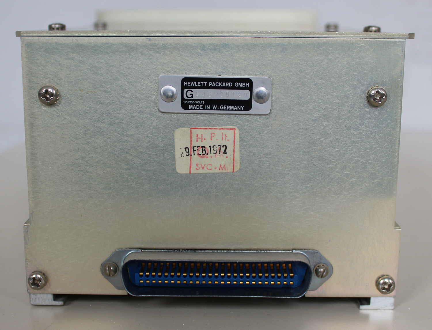
 3305A SWEEP PLUG-IN per il 3300A FUNCTION GENERATOR della HEWLETT PACKARD GMBH. Matr. N° G 348-00120. Quarta parte.
Nell’inventario per reparto N° 7 di Elettronica, in data febbraio 1968, al n° D 4236 si legge: “A FUNCTION GENERATOR S. 3300 A – HP” ; e la n° D 4236 si legge: “A AUXILIARY PLUG-IN 3301 – HP”, ma forse si tratta del mod. 3305!
È facile trovare le istruzioni in internet agli indirizzi elencati sotto.
http://bee.mif.pg.gda.pl/ciasteczkowypotwor/HP/3300A.pdf
http://hpmemoryproject.org/wb_pages/wall_b_page_10c.htm
http://www.kennethkuhn.com/students/ee431/mfg_data/hpj_nov_1965.pdf
http://www.hpl.hp.com/hpjournal/pdfs/IssuePDFs/1968-05.pdf
Quel che segue è tratto dalle istruzioni della H-P conservate nella Sezione Elettronica.
Il testo prosegue dalla terza parte.
§§§
«4–41. SUMMING AMPLIFIER/COMPARATOR ASSEMBLY.
4-42. The setting of the START and STOP potentiometers determine how much of each ramp is applied to the Summing Amplifier. The sum of these voltages at any point in time determines the output of the Summing Amplifier. The Summing Amplifier output is coupled to the Log Shaper input. It is also coupled to the -l0 Volt Comparator input.
4-43. When the input to the -10 volt comparator is between 0 volts and -10 volts, A4Q8A is saturated, holding A4Q9 off. When the input is between -10 volts and -20 volts, A4-Q8A is turned off. A4Q9 is now saturated, furnishing current through ASRS to the Log Shaper input.
4-44. When the Summing Amplifier output is between 0 volts and -10 volts, A4Q10 is conducting. Field effect transistor (FET) A4Q11 is also conducting, which puts a short circuit in parallel with A1C1 and its padding capacitors. When the Summing Amplifier output is between -10 volts and -20 volts A4Q10 is turned off, opening the FET A4Q11. The short circuit is now removed from the A1 [1A] capacitor group, putting it in series with the main capacitor group A1 [1]. This reduces the integrating capacitance by a factor of 100 at the same time that the Log Shaper input current is reduced by a factor of 100. As shown by the formula in Paragraph 4-10:
f = i/2cAe
there is no change in frequency at this switch-point. The capacitor groups [1] and [1A] are used only in the low frequency range, but the same principle also applies in the other two ranges.
4-45. In MANUAL and EXT FREQ CONTROL A4Q13 is always cut off. In AUTO and TRIG A4Q13 conducts from T3 to T4. When conducting, A4Q13 prevents A4Q10 from turning on FET A4Q11 at T3. At T2 A4Q14 turns on FET A4Q12, which discharges capacitor group [1A]. A4R47 limits the discharge current through A4Q12. At T4, A4Q11 turns on and A4Q12 turns off. Capacitor group [1A] is now shorted out of the circuit again.
4-46. LOG SHAPEH ASSEMBLY.
4-47. Paragraphs 4-47 though 4-51 refer to Schematic Diagram 3, Figure 7-4. Mode of operation is AUTO, sweeping up through a four decade range.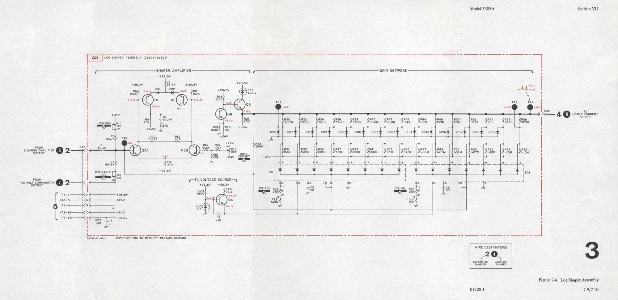 4-48. At T0 the output of the Summing Amplifier applied to the input of the Shaper Amplifier is 0 volts. The shaper output voltage is 0.2 volts. The feedback circuit for the Shaper Amplifier includes the main feedback resistor A5R22, in parallel with all the odd-numbered resistors from A5R31 through A5R59.
4-49. With a 0 volt input, all the parallel feedback resistors are in the circuit, giving the Shaper Amplifier its lowest gain about .093. Gain of the amplifier is found by the basic formula:
A = rf / rin
where rf is total feedback resistance and rin is the input resistance A5Rl. As the input voltage increases, the output voltage increases with a small gain. When the output reaches about 0.52 volts, the first diode in the integrated circuit IC1 becomes back-biased. A5R31 is no longer in parallel with A5R22. The total value of rf is slightly larger; therefore, the gain of the Shaper Amplifier is slightly higher. As the output voltage increases further, the next diodes become back-biased one at a time. This causes the amplification to be increased as each diode stops conducting. The values of the gain network are chosen to give a logarithmic gain to the amplifier. At T1the gain is about 9.3, 100 times greater than at T0, raising the output to +20 volts.
4-50. At T1 the Summing Amplifier, starts furnishing a current through XA5-1 to replace the current being taken out of the Shaper Amplifier input. The total Shaper Amplifier inputs now 0 volts, and the output immediately drops to 0.2 volts. The Shaper Amplifier output again increases logarithmically to +20 volts at T2. A5CR6 through A5CRI9 are each biased so that the reverse bias on each of the integrated circuit diodes is less than one volt. This prevents reverse breakdown of the diodes, and also prevents large leakage currents that would affect the gain of the amplifier.
4-51. A5R2 controls the maximum output voltage of the Shaper Amplifier. A5R5 is adjusted for minimum frequency jump at T1. A5R25 and A5R27 control the internal temperature of the integrated circuit packages.
4-52. LOWER CURRENT SOURCE ASSEMBLY.
4-53. Paragraphs 4-54 through 4-59 refer to Schematic Diagram 4, Figure 7-5.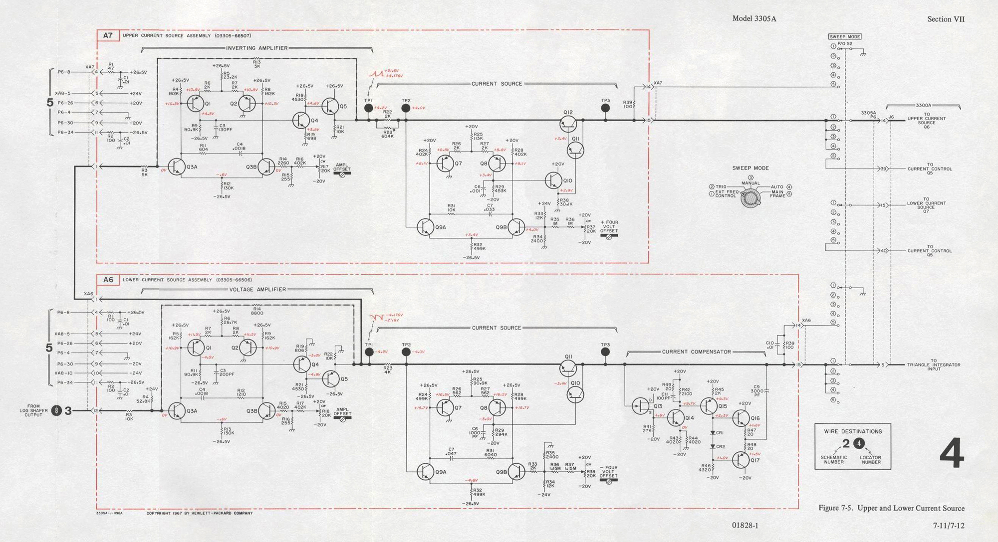 4-54. As the input voltage to the Voltage Amplifier varies from +0.2 volts to +20 volts, the output at A6TP1 varies from -4.176 volts to -21.6 volts. This voltage is coupled to the Current Source and also to the input of the Upper Current Source Assembly.
4-55. The voltage at A6Q9A base is held at -4.000 volts. The Current Source output at A6TP3 varies from 44 microamps to 4.4 milliamps at 4 volts.
4-56. The Current Compensator amplifies the small triangle wave at the integrator input and supplies current equal to the current which is shunted to ground through the 3300A capacitor A13C1. As frequency increases, more current flows to ground through A13C1. The. Current Compensator also couples more current into the -4 Volt Amplifier output as frequency increases, offsetting the current loss through A13C1.
4-57. In MAIN FRAME, A6R39 serves as a voltage dropping resistor, developing a test voltage at A6TP3, which varies from ,0044 volts to .44 volts as the MANUAL sweep vernier is turned through a four decade sweep.
4-58. UPPER CURRENT SOURCE ASSEMBLY.
4-59. The inverting Amplifier has an output varying from +4.l76 volts to +21 .6 volts. The voltage at A7Q9A base is held at +4.000 volts. In MAIN FRAME, the output at A7TP3 varies from 88 microamps to 8.8 milliamps at 4 volts, indicating two times the lower current to the 3300A triangle integrator. In MAIN FRAME the test voltage at A7TP3 varies from .0088 volts to .88 volts.
4-60. POWER SUPPLY ASSEMBLY.
4-61. Paragraphs 4-61 through 4-64 refer to Schematic Diagram 5, Figure 7-6.
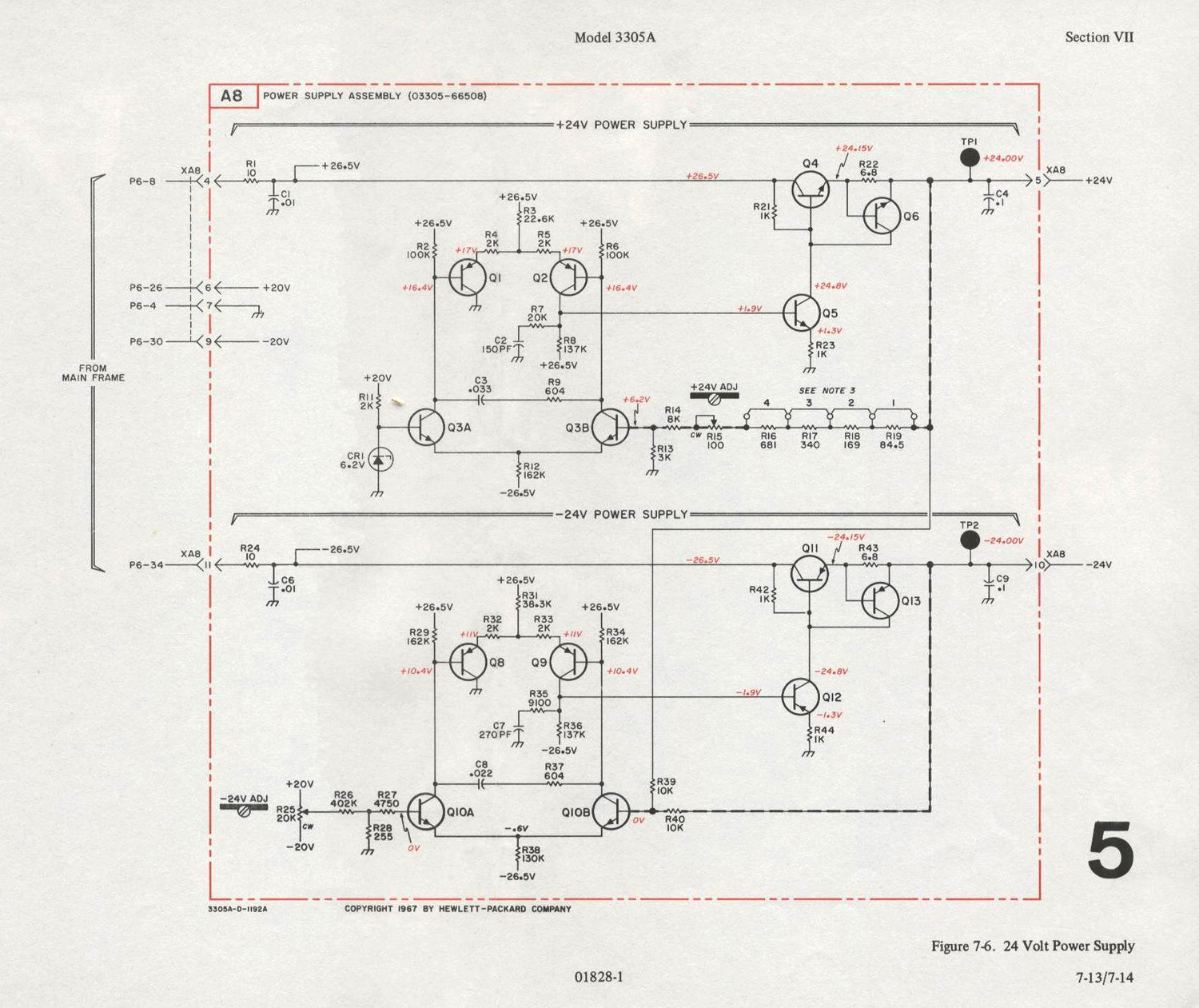 4-62. All voltages required by the 3305A are supplied by the 3300A power supply with the exception of the +24 volts and the -24 volts.
4-63. The +24 volt power supply uses a 6.2 volt zener diode A8CR1 as a reference. A8Q1, A8Q2, A8Q3A and A8Q3B make up a differential amplifier which uses the zener diode as reference. A8R13 through A8R19 make up a voltage divider feedback network. A8RI6 through A8R19 are +24.000 volts at A8TP1. Refer to Paragraph 5-56 for adjustment procedure necessary when A8CR1 is replaced.
4-64. The +24.000 is coupled from the +24 volt power supply output to A8R39 is matched with feedback resistor A8R40, causing the -24 volt output to follow the +24 volt output».
§§§
Omettiamo la Sezione V: Manutenzione, per la sua meticolosa lunghezza, ma riportiamo le relative figure e tabelle.
Continua nella quinta parte.
Per consultare le altre schede scrivere “3305A” su Cerca. Per consultare le schede del generatore di funzioni 3300A scrivere “3300A”.
Foto di Claudio Profumieri, elaborazioni e ricerche di Fabio Panfili.
Per ingrandire le immagini cliccare su di esse col tasto destro del mouse e scegliere tra le opzioni.