 Variable Phase Function Generator, Model 203A, Hewlett Packard. Prima parte.
Per cause indipendenti dalla nostra volontà non disponiamo dell’inventario generale dell’epoca.
Nell’inventario per reparto N° 7 di Elettronica, in data febbraio 1968, al n° D 4224 si legge: “Function Generator 203/A”. Ma ce ne sono due esemplari; l’altro costruito dalla Yokogawa Hewlett Packard viene presentato nella seconda parte.
In rete si trovano vari documenti, manuali di istruzioni e altre informazioni ai seguenti indirizzi:
http://hparchive.com/Manuals/HP-203A-Manual-sn425.pdf
http://www.hpl.hp.com/hpjournal/pdfs/IssuePDFs/1965-07.pdf
Presso la Sezione Elettronica è conservato il manuale di istruzioni nel quale si trovano note e disegni aggiunti a matita delle riparazioni fatte negli anni.
Noi le abbiamo tolte per ridare ai disegni l’aspetto originale.
Quel che segue è parte delle istruzioni.
Abbiamo omesso il capitolo MAINTENANCE, pur pubblicandone alcune figure che riteniamo significative, ed altre parti.
 §§§
§§§ «SECTION I
GENERAL INFORMATION
1-1. DESCRIPTION.
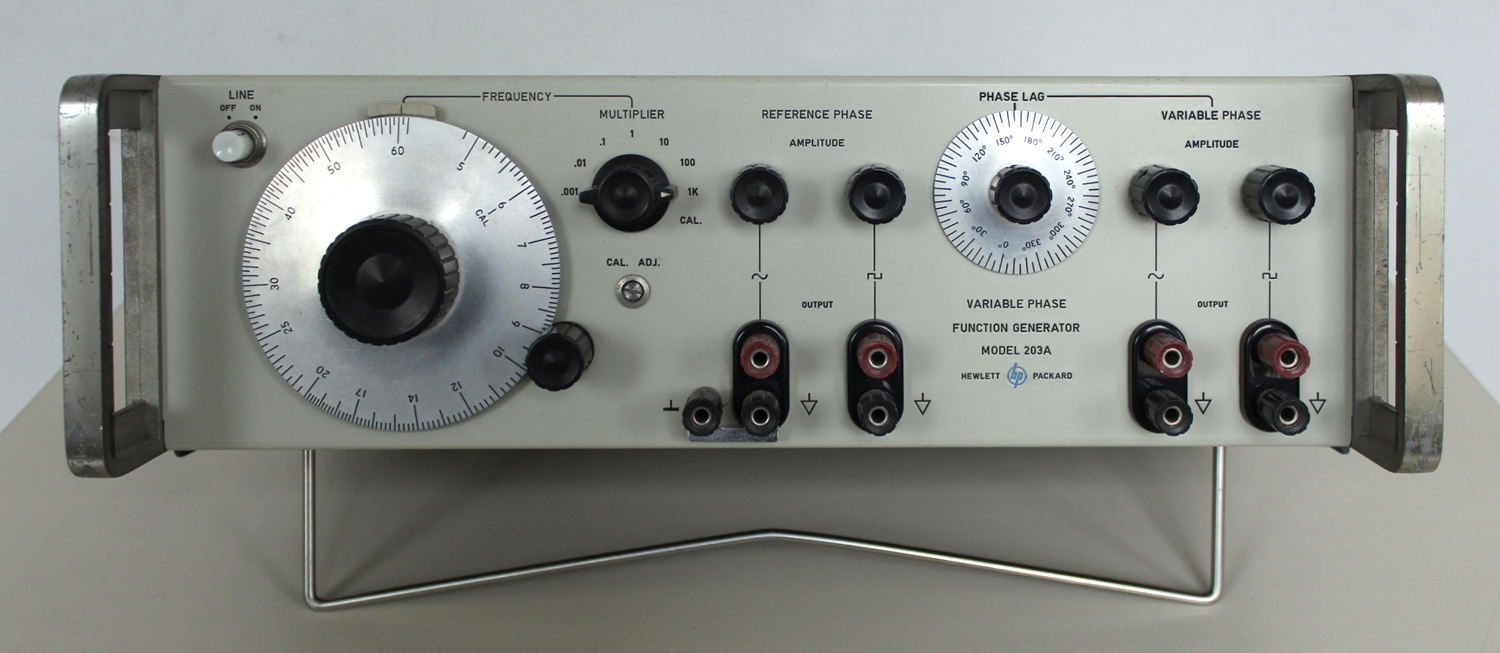
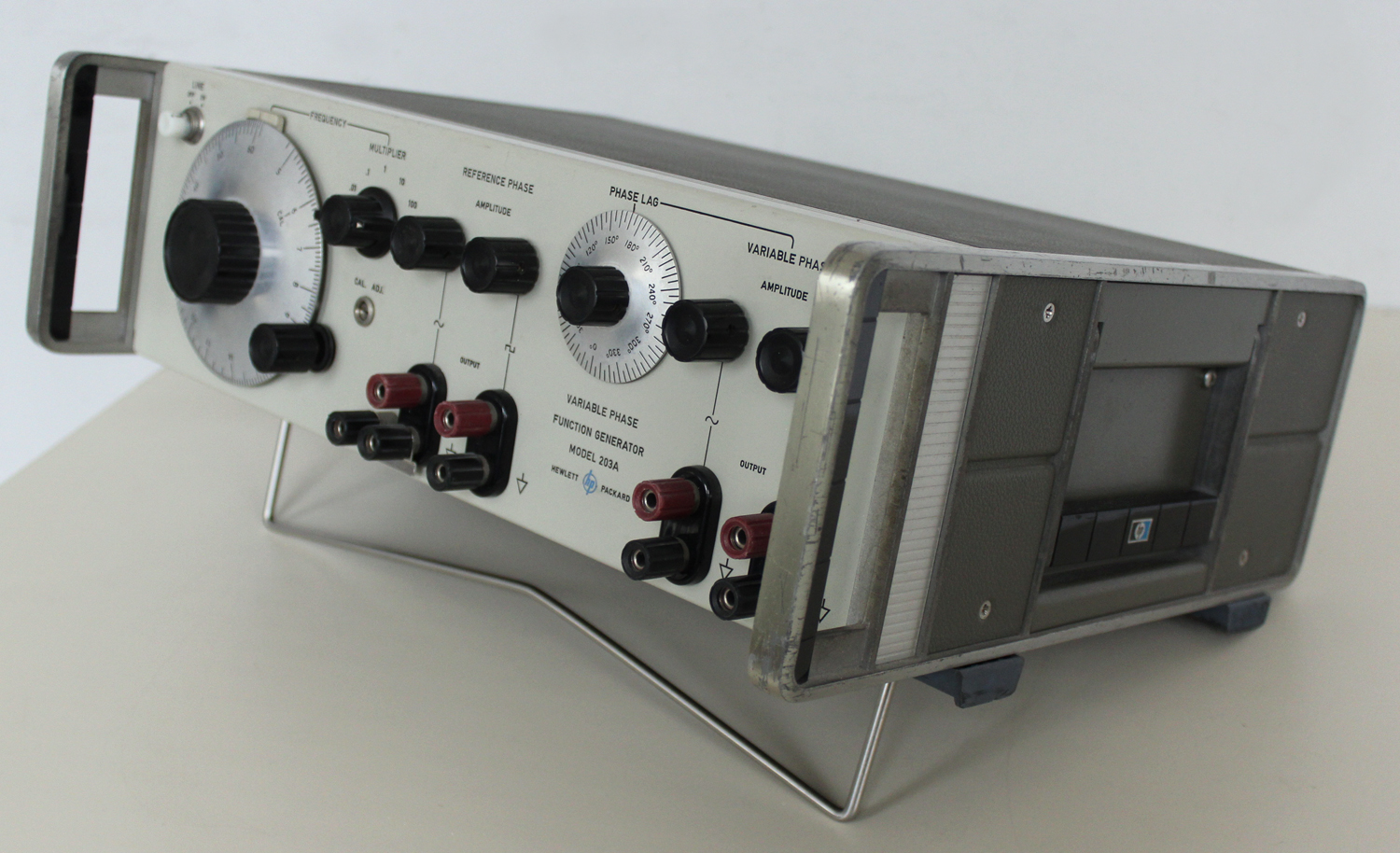
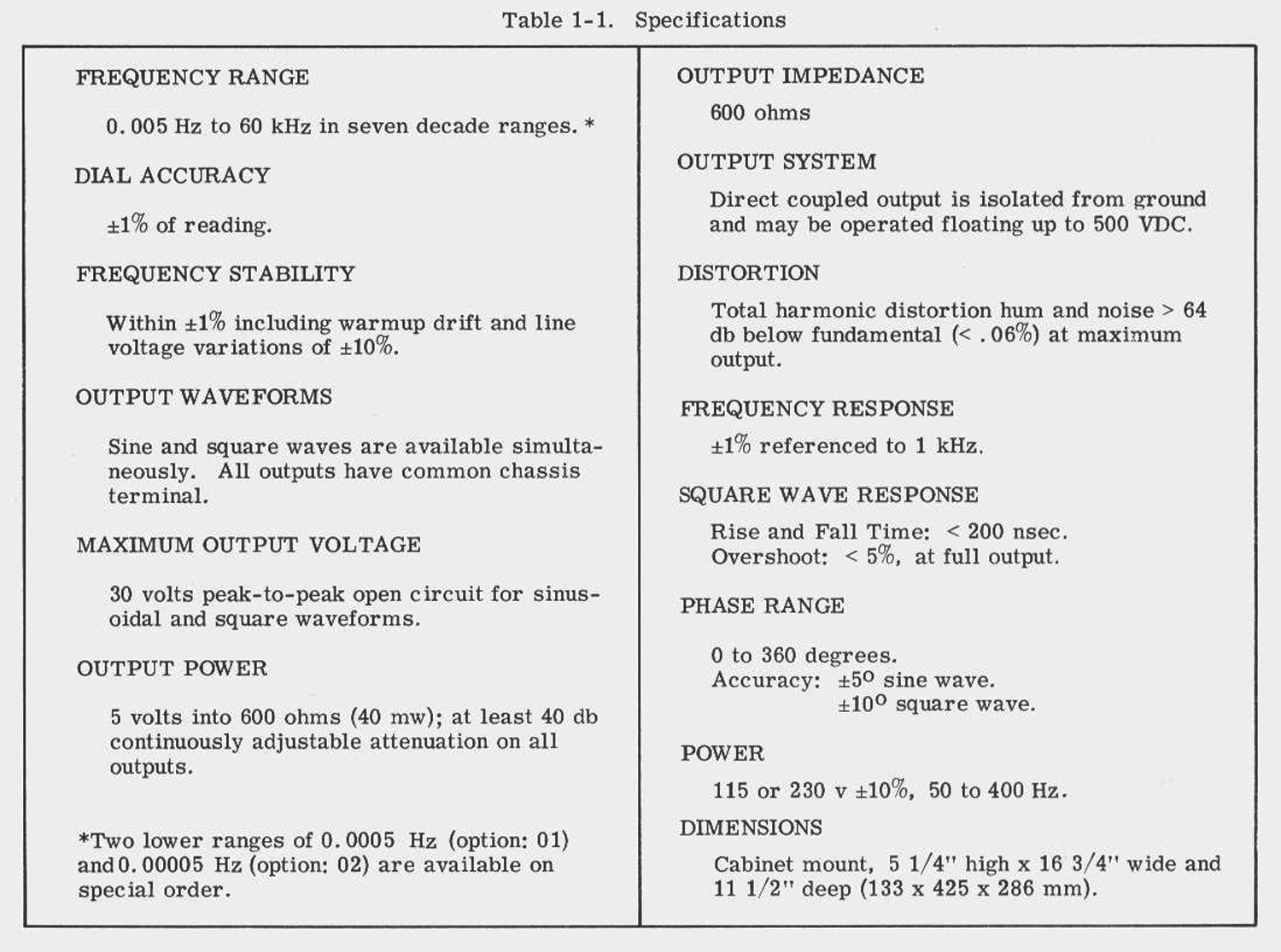
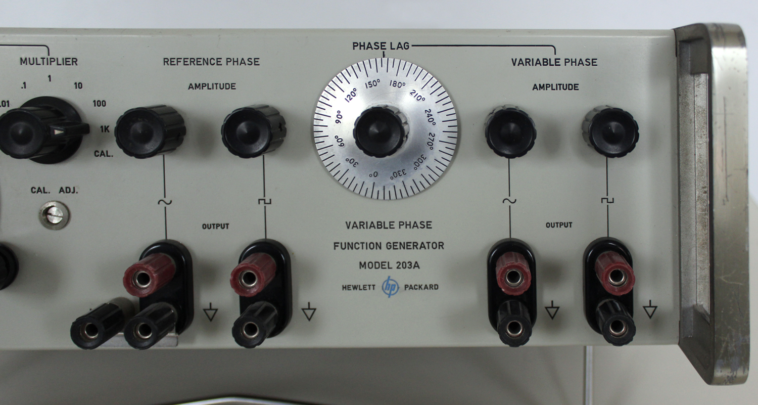
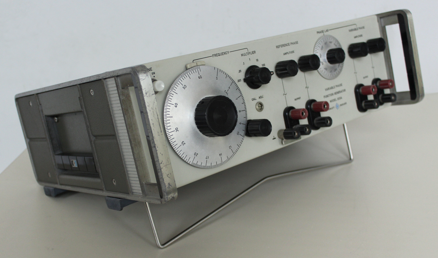
1-2. The Hewlett-Packard Model 203A Variable Phase Function Generator is a low frequency function generator which provides two sine wave and two square wave test signals at frequencies from 0.005 cps to 60 kc. (Refer to paragraph 1-5, Options Available).
1-3. The four test signals are provided at the front panel OUTPUT connectors at an open circuit signal level of 30 volts peak-to-peak. The sine wave and square wave test signals provided at the REFERENCE PHASE OUTPUT connectors are fixed in phase and provide a reference phase for the test signals at the VARIABLE PHASE OUTPUT connectors. The variable phase test signals are continuously variable from 0° to 360° lag with respect to the phase of the reference test signals. The amplitude of the four output signals can be varied with individual continuously variable 40 db attenuators (AMPLITUDE controls).
1-4. The output terminals are floating with respect to ground and can be used to supply an output voltage with the common terminal grounded or can be floated up to 500 volts dc above chassis ground. The output impedance for all four test signal outputs is 600 ohms.
1-5. OPTIONS AVAILABLE.
1-6. Options 01 and 02 are available to provide two additional frequency ranges to the Model 203A. Option 01 includes one additional Decade Module Board Assembly which extends the lower limit of the frequency range from 0.005 cps to 0. 0005 cps. Option 02 includes two additional Decade Module Board Assemblies which extend the lower limit of the frequency range from 0. 005 cps to 0. 00005 cps. These two options can also be installed as a field modification (see Section VI for stock number of Decade Module Board Assemblies).
1-7. APPLICATIONS.
1-8. The Model 203A can be used for phase shift measurements, vibration studies, servo applications, medical research, distortion measurements, geophysical problems, subsonic and audio testing.
1-9. INSTRUMENT IDENTIFICATION.
1-10. Hewlett-Packard uses a two-section nine character (0000A00000) or eight character (000-00000 or 000A00000) serial number. The first three or four digits (serial prefix) identify a series of instrument; the last five digits identify a particular instrument in that series. A letter placed between the two sections identifies the country where the instrument was manufactured. The serial number appears on a plate located on the rear panel. All correspondence with Hewlett-Packard Sales/Service Offices with regard to an instrument should refer to the complete serial number.
1-11. If the serial prefix does not agree with the serial prefix on the title page of this manual, a “Manual Changes” sheet supplied will describe changes which will adapt this manual to an instrument with a different serial prefix. Technical corrections (if any) to this manual, due to known errors in print, are called Errata and are shown on the change sheet. For information on manual coverage of any hp instrument, contact the nearest hp Sales/Service Office (addresses are listed at the rear of this manual).
SECTION II
INSTALLATION
2-1. INSPECTION.
2-2. This instrument was carefully inspected both mechanically and electrically before shipment. It should be physically free of mars or scratches and in perfect electrical order upon receipt. To confirm this, the instrument should be inspected for physical damage in transit. Also check for supplied accessories, and test the electrical performance of the instrument using Table 2-1 or the procedure outlined in paragraph 5-3. If there is any apparent damage, file a claim with the carrier and refer to the warranty on the inside front cover of this manual.
2-3. POWER REQUIREMENTS.
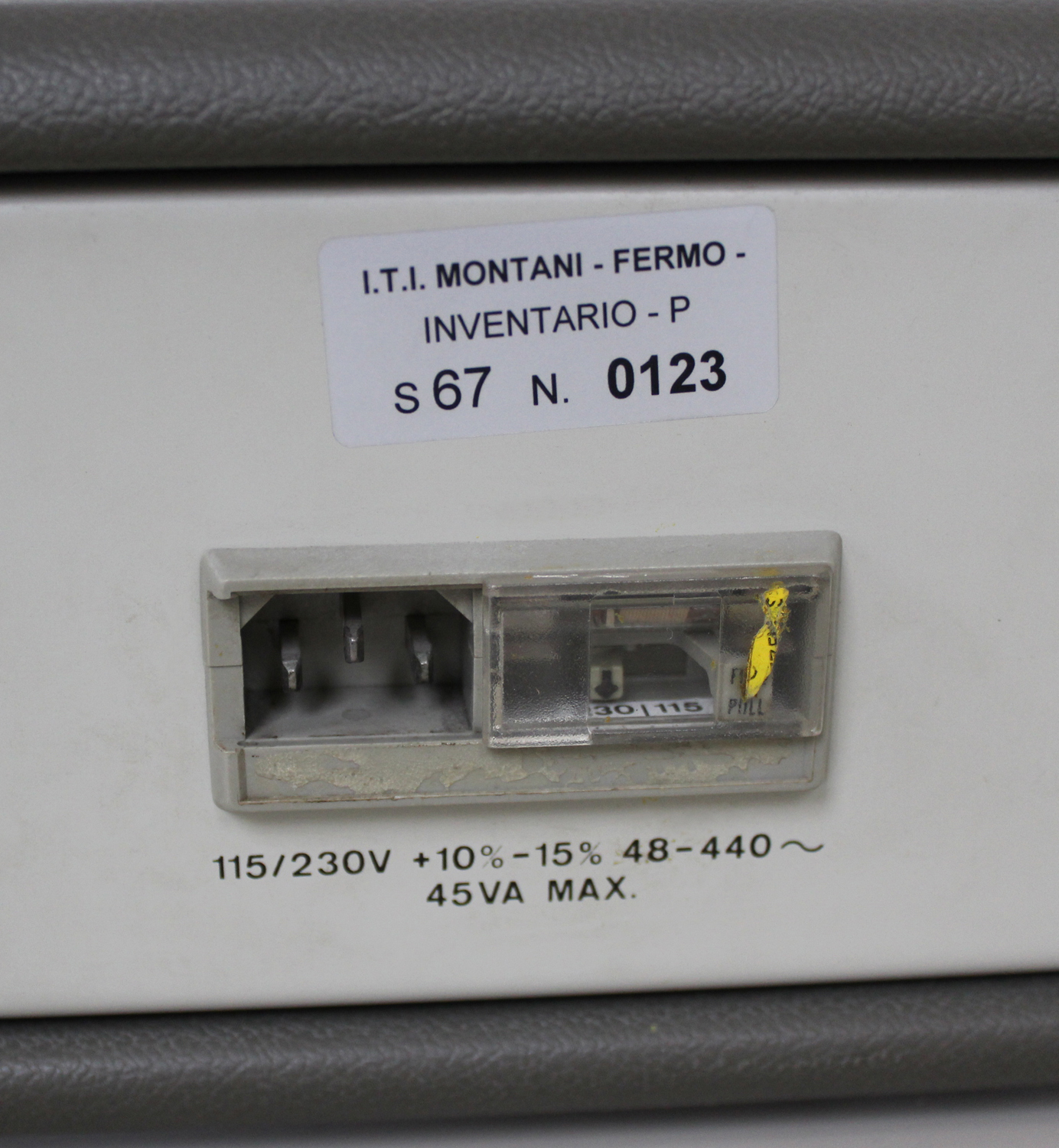
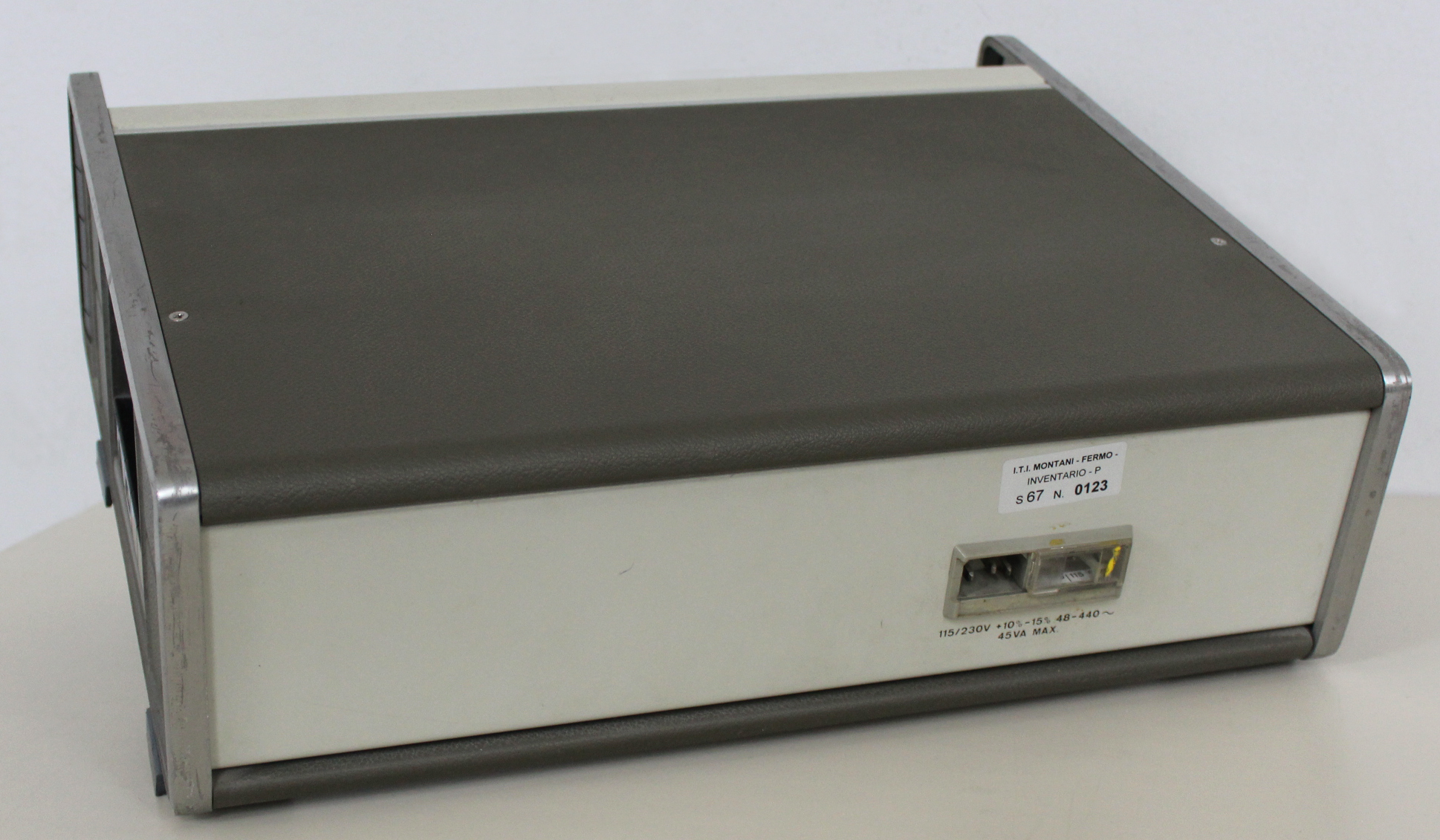
2-4. The Model 203A will operate from either 115 or 230 vac, 50 – 400 Hz. The instrument can be easily converted from 115 to 230 volt operation by changing the position of the slide switch, located on rear panel, so that the designation appearing on the switch matches the nominal voltage of the power source.
2-5. THREE-CONDUCTOR POWER CABLE.
2-6. To protect operating personnel, the National Electrical Manufacturers Association (NEMA) recommends that the instrument panel and cabinet be grounded. All Hewlett-Packard instruments are equipped with a three-conductor power cable which, when plugged into an appropriate receptacle, grounds the instrument. The offset pin on the power cable three-prong connector is the ground wire.
2-7. To preserve the protection feature when operating the instrument from a two-contact outlet. use a three-prong to two-prong adapter and connect the green pigtail on the adapter to ground.
2-8. INSTALLATION.
2-9. The Model 203A is fully transistorized; therefore no special cooling is required. However, the instrument should not be operated where the ambient temperature exceeds 55 °C (131 °F).
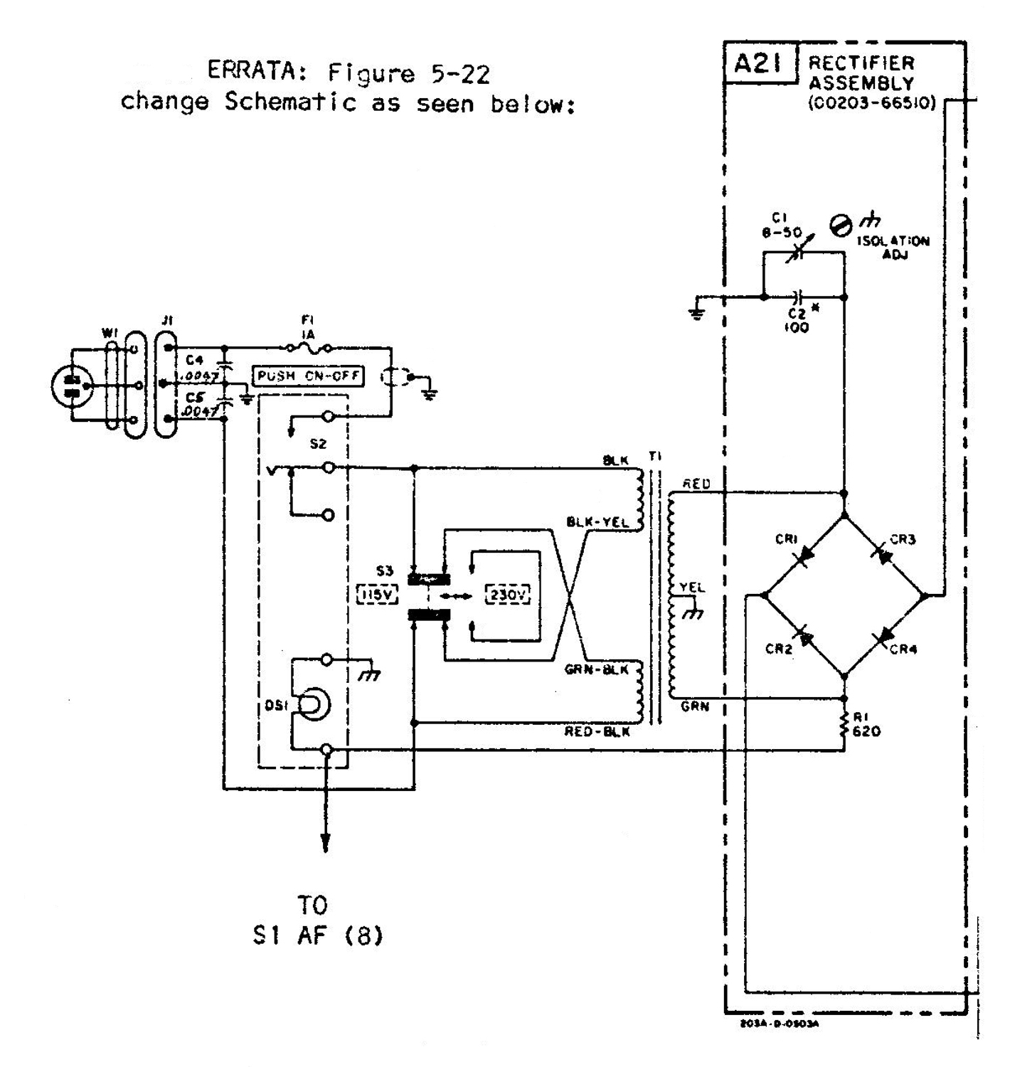
OMISSION: from par. 2.10 at par. 2.13 (editor’s note).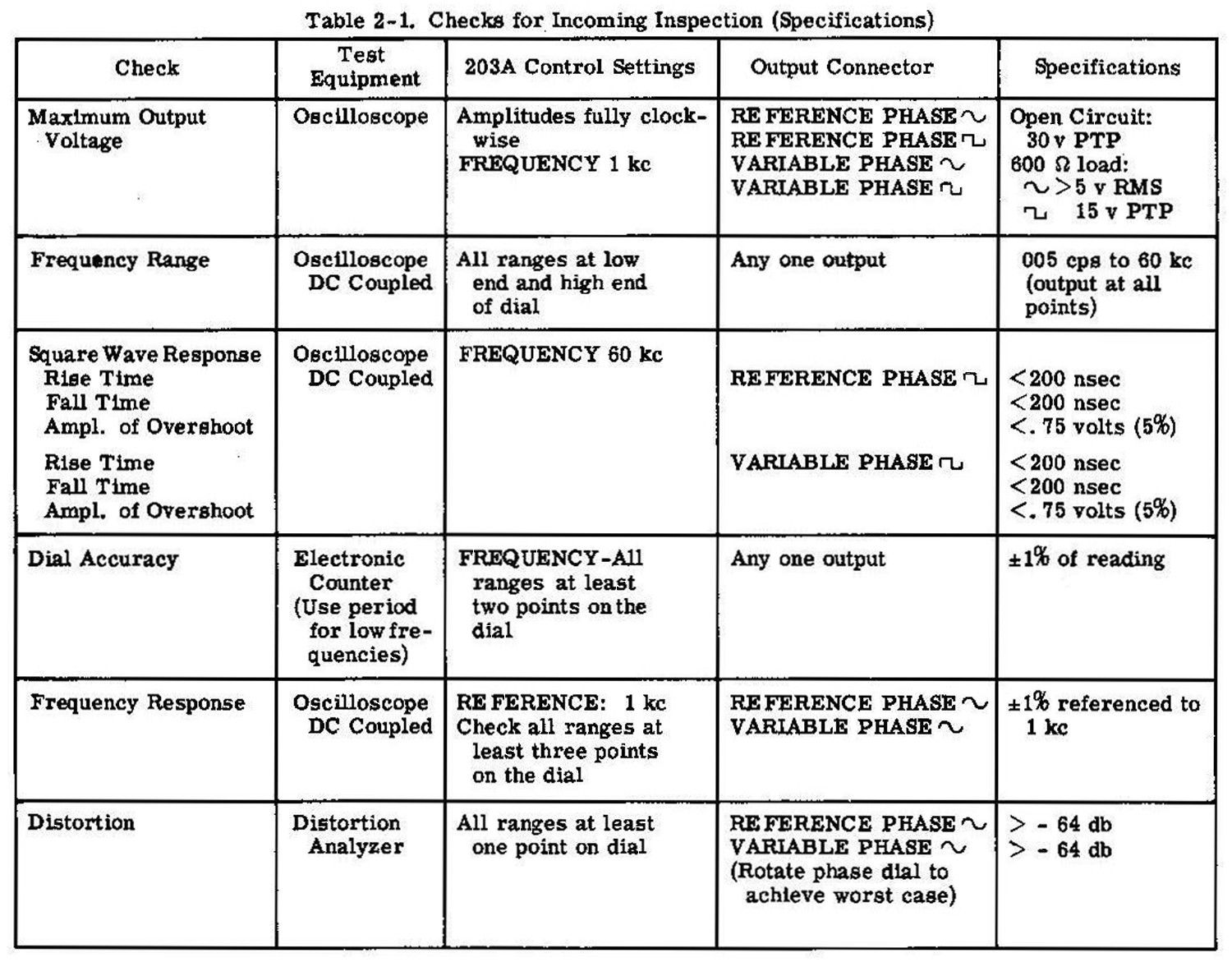 SECTION III OPERATION
3-1. INTRODUCTION.
3-2. The Model 203A generates two sine wave and two square wave signals which are available simultaneously at the front panel OUTPUT connectors. The output signal frequency is determined by the position of the FREQUENCY dial and FREQUENCY MULTIPLIER switch. By the use of the PHASE LAG control, the phase of the VARIABLE PHASE OUTPUT signals (one sine wave and one square wave) can be continuously adjusted from 0° to 360° with respect to the REFERENCE PHASE OUTPUT Signals. The OUTPUT terminals provide an open-circuit signal level of 30 volts peak-to-peak. The individual AMPLITUDE controls provide 40 db of attenuation for each output signal. The CAL ADJ control provides a means of calibrating the FREQUENCY dial with the line frequency.
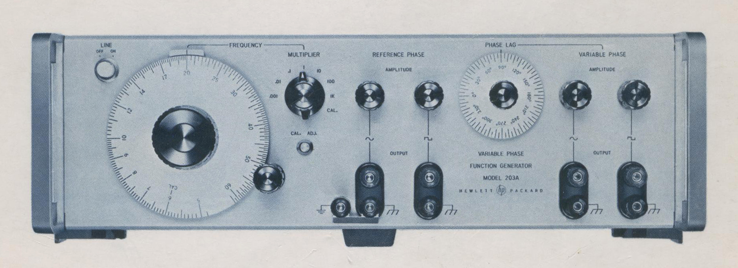
3-3. CONTROLS AND INDICATORS.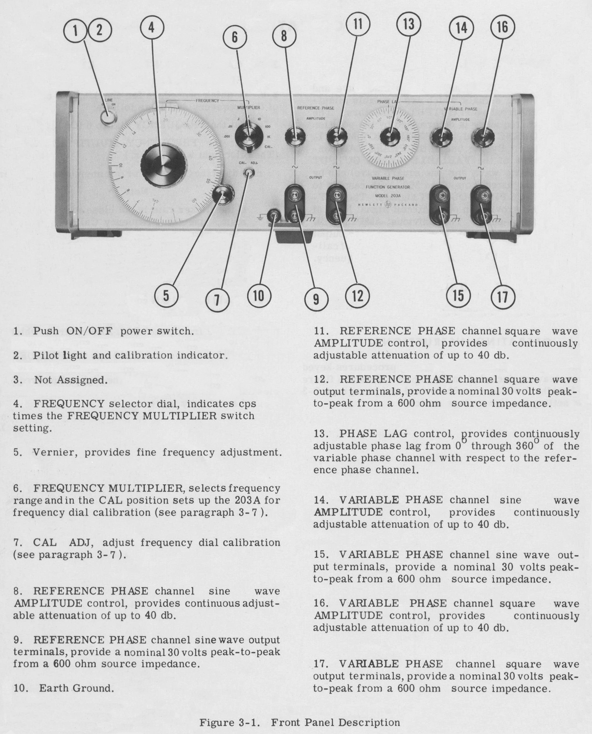 3-4. Figure 3-1 describes the function of all front panel controls, connectors, and indicators. The description of each component is keyed to a drawing which is included within the figure.
3-5. OPERATING INSTRUCTIONS.
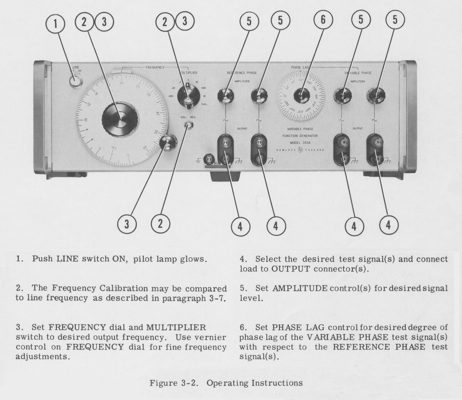 3-6. Figure 3-2 contains operating procedures keyed to a drawing included in the figure. Refer to figure 3-1 for the function of each control and paragraph 2-3 for setting the line voltage switch.
3-7. CALIBRATION FOR 60 CYCLE LINE FREQUENCY.
3-8. A quick procedure for checking the calibration of the frequency dial is as follows:
a. Set the FREQUENCY dial to 6 (CAL).
b. Set the FREQUENCY MULTIPLIER to CAL. (The pilot light will flicker. ).
c. Adjust the CAL ADJ for minimum rate of flicker.
Note
If the flicker rate is not close to minimum, use the Frequency Calibration check paragraph 5- 5. When the FREQUENCY MULTIPLIER switch is in the CAL position, there is no output at the REFERENCE PHASE OUTPUT connector.
3-9. CALIBRATION FOR LINE FREQUENCIES OTHER THAN 60 CYCLES.
3-10. For line frequencies other than 60 cps the FREQUENCY dial is set to 1/10 of the line frequency (40 to 400 cps line frequency). Again the calibration is made with the front panel CAL ADJ control, which is adjusted for a minimum flicker rate of the pilot lamp. For line frequencies above 600 cps the FREQUENCY dial is set to 1/30 of the line frequency (33.3 for a 1000 cps line frequency). At the higher line frequencies the flicker intensity decreases and the CAL ADJ control sensitivity increases.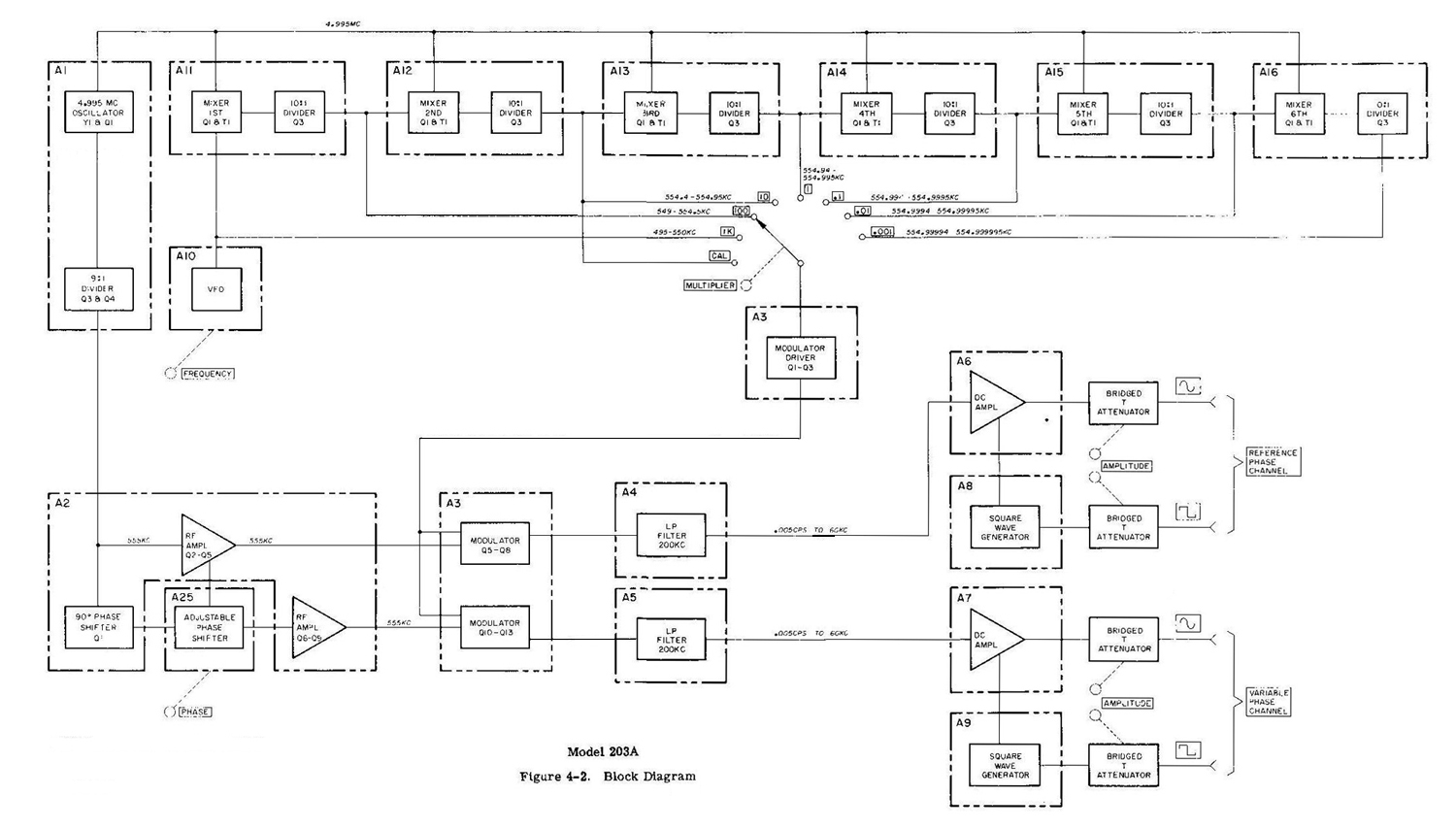 SECTION IV
PRINCIPLES OF OPERATION
4-1. OVERALL DESCRIPTION.
4-2. This section describes how the Model 203A Variable Phase Function Generator operates. The block diagram, figure 4-2, shows the main sections and the signal flow within the Model 203A.
4-3. The Model 203A is a beat-frequency oscillator which, by mixing two high-frequency signals, generates signals in the frequency range of 0.005 cps to 60 kc (refer to paragraph 1-5 for options). One of the high-frequency signals is a fixed frequency; the other is variable. The Model 203A has two signal channels, REFERENCE PHASE and VARIABLE PHASE, each of which produces a sine-wave signal and a square-wave signal. The two channels are electrically similar except that the VARIABLE PHASE channel contains a continuously adjustable phase-shifting circuit which changes the phase relationship of the VARIABLE PHASE OUTPUT with respect to the REFERENCE PHASE OUTPUT. The four signals (two reference phase and two variable phase) are available simultaneously at the OUTPUT connectors.
4-4. The fixed frequency signal, which is generated by a crystal oscillator, is applied to both channels and routed to a modulator through an RF Amplifier within each channel. The variable frequency signal is applied directly to the modulator of each channel. The frequency of the variable frequency signal is controlled by the position of the FREQUENCY dial and the setting of the FREQUENCY MULTIPLIER switch. These two signals are mixed in the modulator and the difference in frequency between the two signals is the output frequency of the Model 203A.
4-5. CRYSTAL OSCILLATOR AND DIVIDER ASSEMBLY (A1).
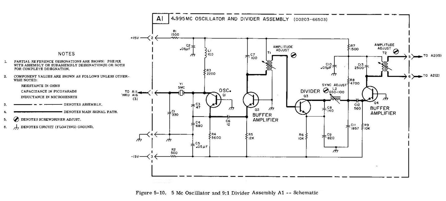 4-6. Assembly A1 consists of a crystal controlled oscillator and a 9:1 frequency divider. Refer to the schematic diagram, figure 5-10, for circuit details.
4-7. CRYSTAL OSCILLATOR.
4-8. The oscillator (A1Y1 and A1Q1) is a crystal controlled grounded base Colpitts oscillator. The 5 Mc output is applied through buffer amplifier A1Q2, for isolation, to the base of the 9:1 frequency divider.
4-9. 9:1 FREQUENCY DIVIDER.
4-10. The 9:1 divider consists of a divider A1Q3 and a tank circuit which consists of A1C8, A1C9, A1C11, and A1L2. The divider is basically a class C grounded base Colpitts oscillator.
4-11. Two things occur during each cycle of the divider operation. One is amplitude modulation of the signal applied to the base of A1Q3, and the second is a mixing action within A1Q3. Each function occurs at a different time during each cycle of oscillation and together tend to synchronize A1Q3 with a sub-multiple frequency of the frequency applied to the base of the divider.
4-12. Divider A1Q3 operates in the region of voltage saturation for a portion of each cycle. During the saturation period, the impedance between the base and collector of A1Q3 becomes very low; for the rest of cycle the impedance between the base and collector is relatively high. The variation in impedance between base and collector of A1Q3 results in amplitude modulation (about 10%) of the signal on the base of the divider. This amplitude modulation creates sidebands at the 8th and 10th harmonic of the divider oscillating frequency.
4-13. The signal applied to the base of A1Q3 is about 4.995 Mc which is generated by the crystal oscillator circuit. The tank circuit of the 9:1 divider is tuned so that A1Q3 is oscillating at the 9th sub-multiple frequency of 4.995 Mc (555 kc).
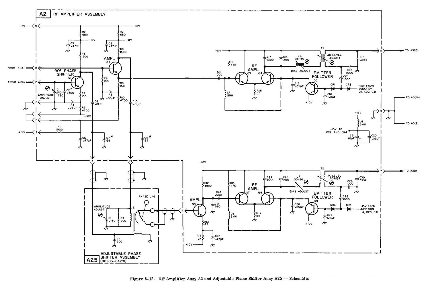
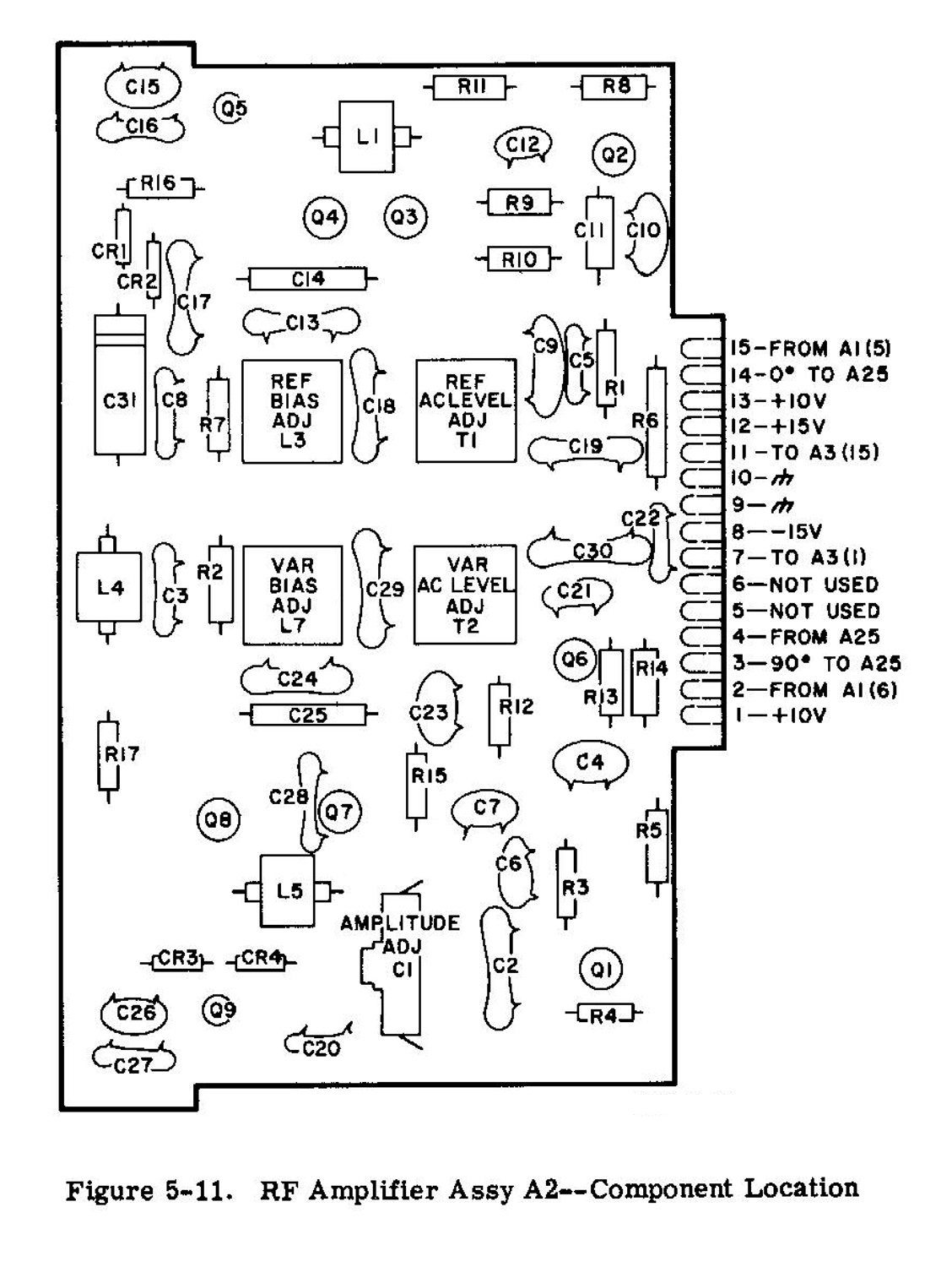
4-14. The mixing-process within A1Q3 occurs at the time during each cycle when the divider just starts to conduct. During this short time, the 8th and 10th harmonic of the 555 kc signal are mixed with the 9th harmonic resulting in a frequency component at 555 kc which influences the oscillations of A1Q3. The result is that A1Q3 stays synchronized to the 9th sub-harmonic of 4.995 Mc. 4-15. The pi type tank circuit filters out harmonic frequencies which may be present at the collector of A1Q3. A buffer amplifier A1Q4 provides further filtering, isolation, and power gain. The output of the 9:1 divider is a 555 kc signal and is coupled by A1T2 to A2Q1 and A2Q2 (see figures 5- 10 and 5-12)».
 Per consultare la seconda parte scrivere “203A” su Cerca.
Foto di Claudio Profumieri, elaborazioni e ricerche di Fabio Panfili.
Per ingrandire le immagini cliccare su di esse col tasto destro del mouse e scegliere tra le opzioni.

Istituto Tecnico Tecnologico Montani