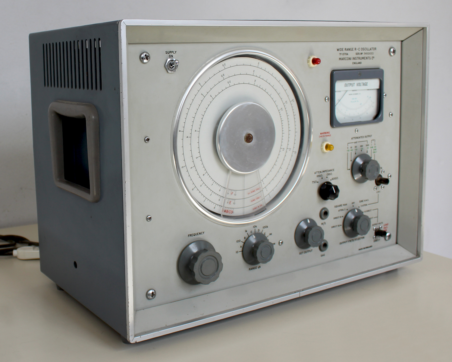
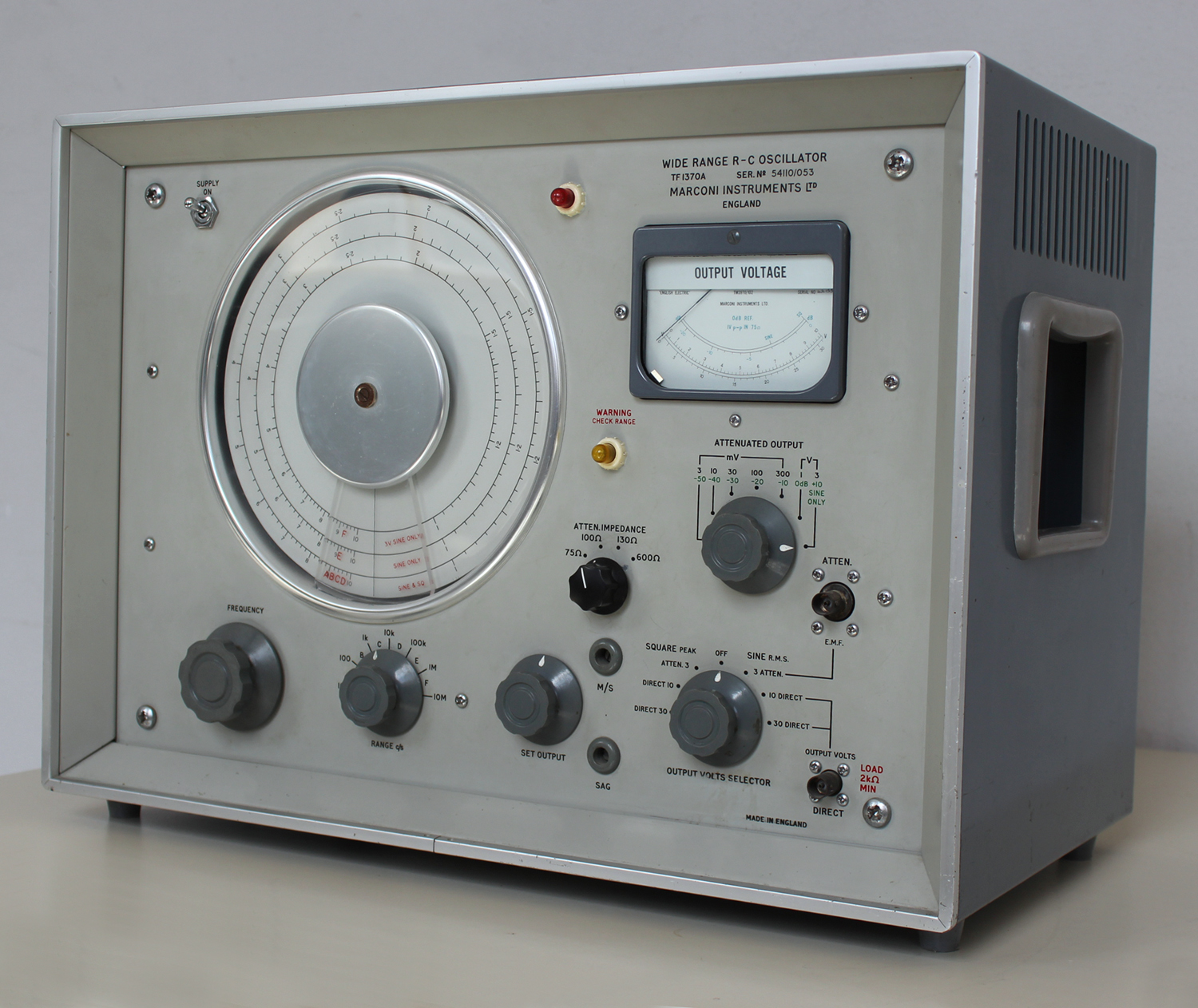
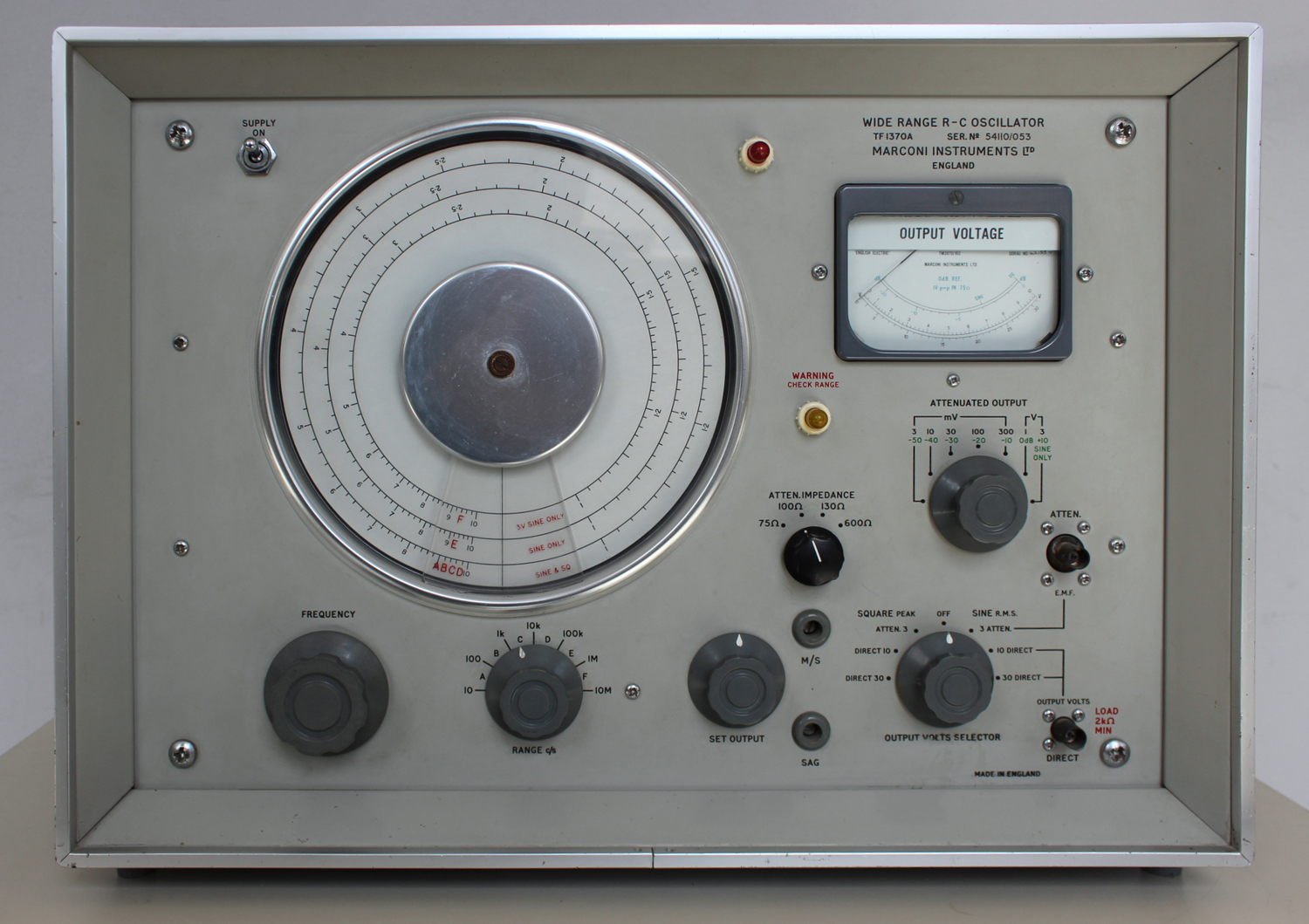
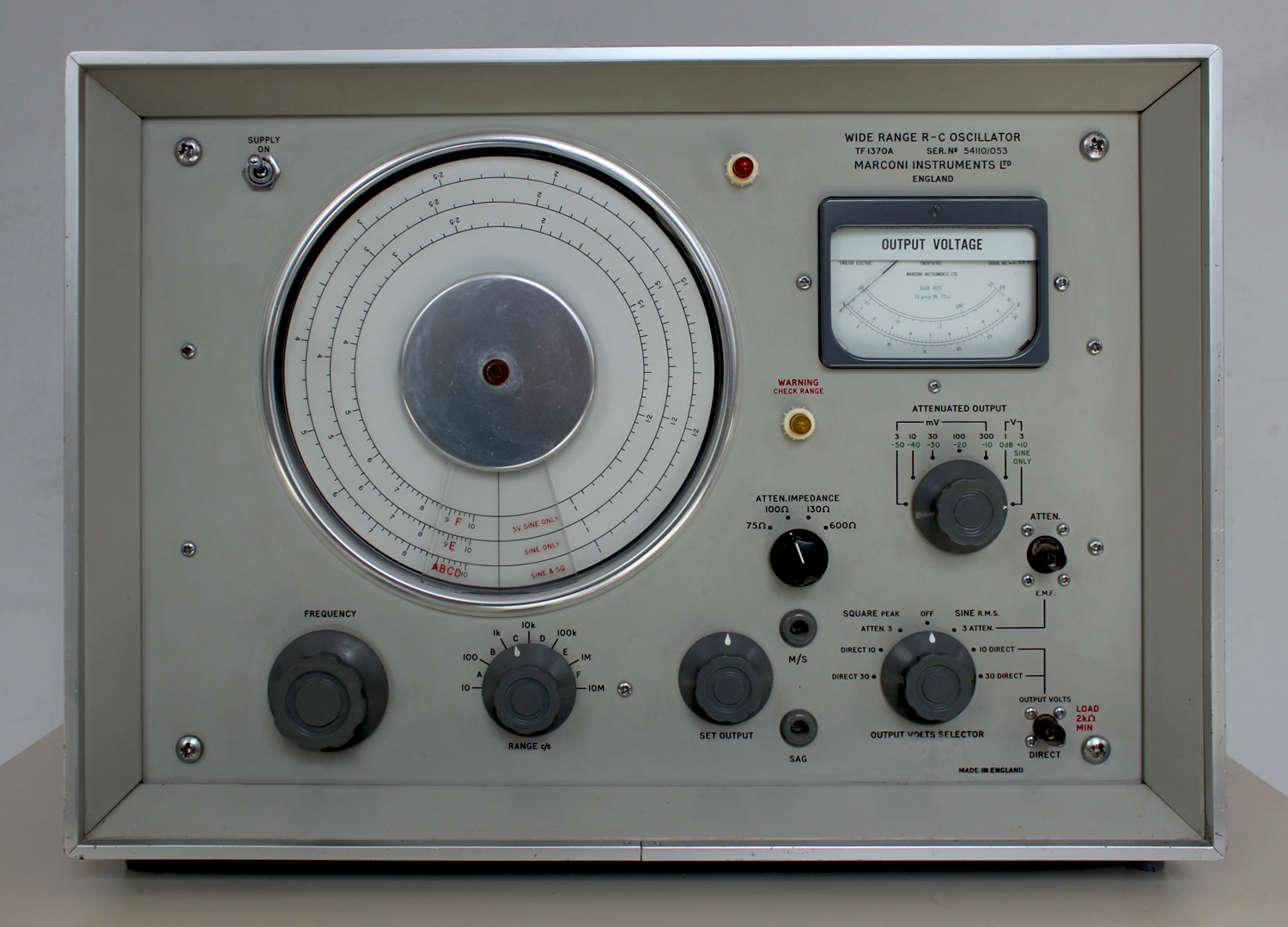
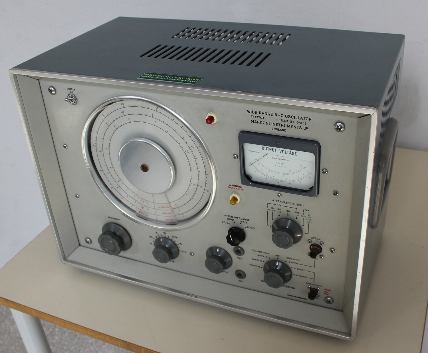
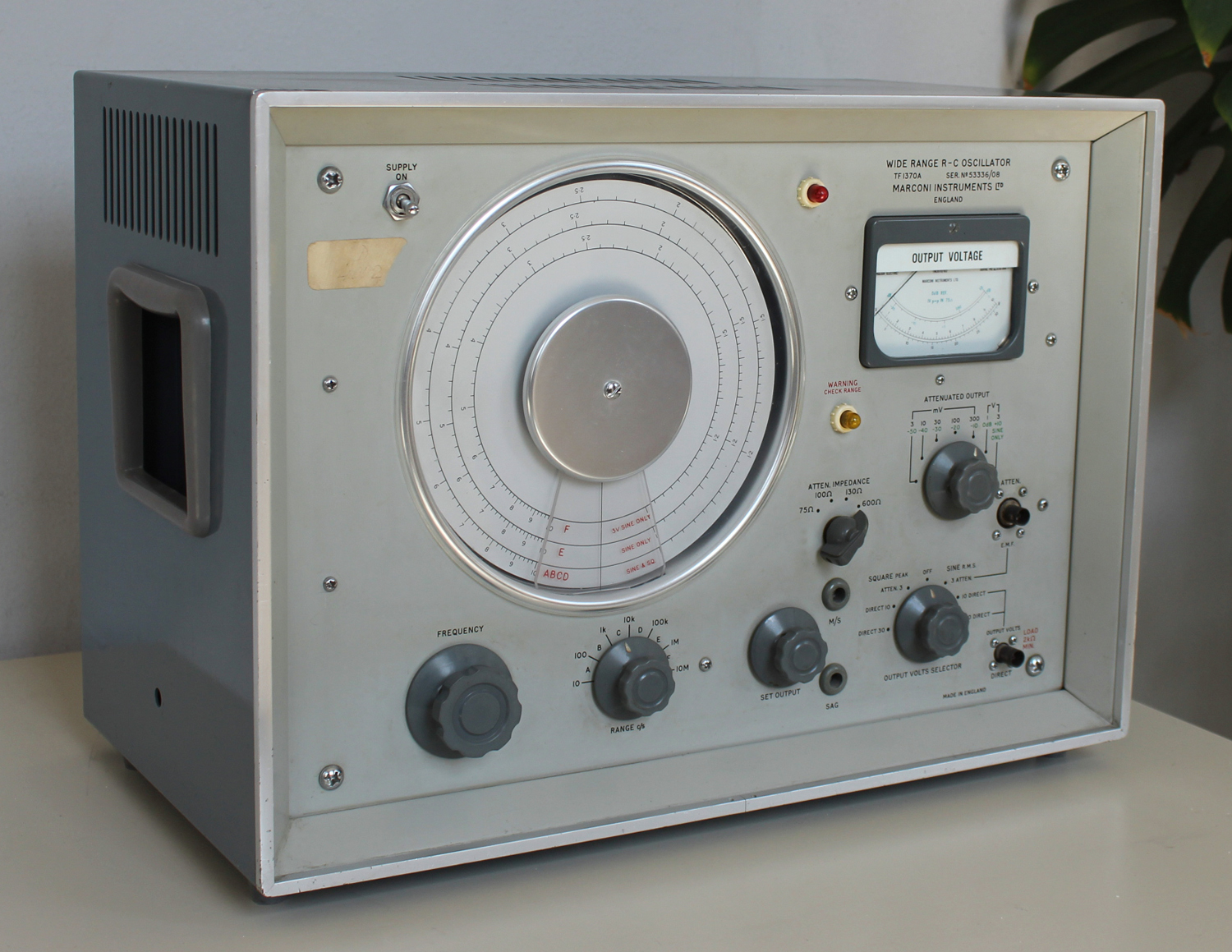
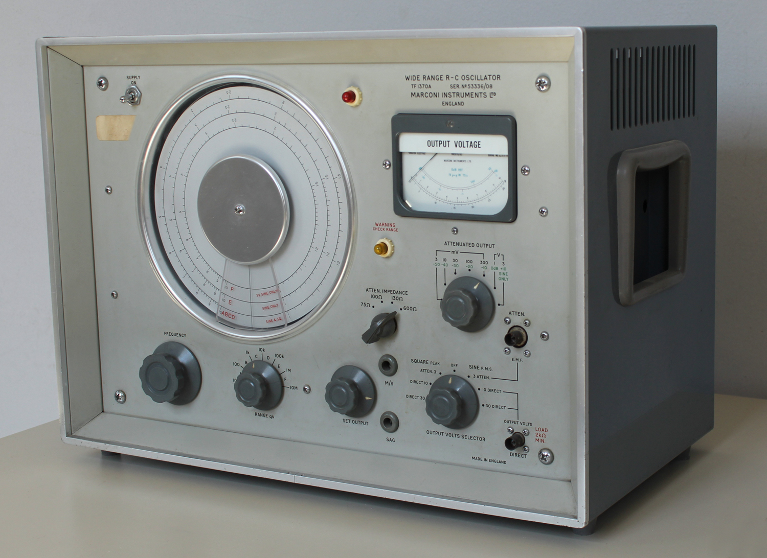
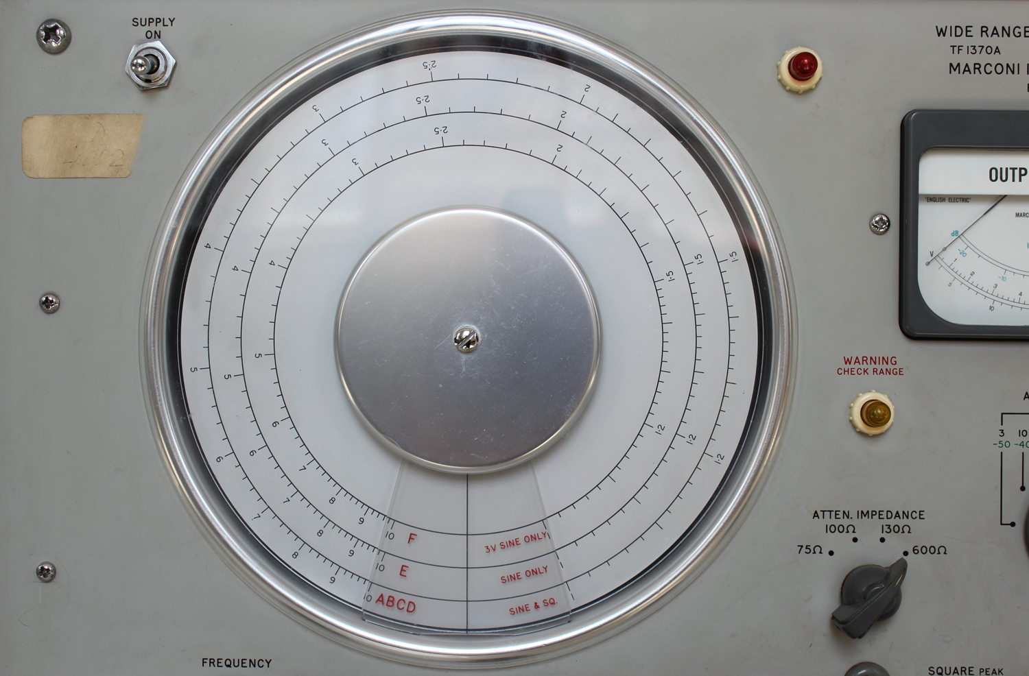
 Wide Range R-C Oscillator TF 1370A, Serial N° 54110/053. Marconi Instruments Ltd. England.
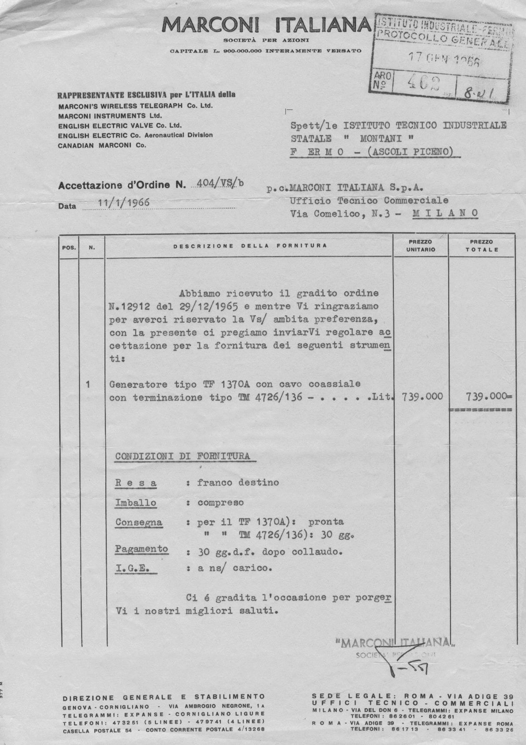
Per ragioni indipendenti dalla nostra volontà per ora non possiamo accedere all’inventario dell’epoca, pur sapendo che si trova al n° 4025 ed è stato acquistato dopo l’esemplare Serial N° 53336/08 e comunque nel 1966.
Il testo che segue è una parte del manuale di istruzioni custodito nell’archivio della Sezione Elettronica.
Una parte precedente del manuale è riportata nella scheda relativa al Wide Range R-C Oscillator TF 1370A, Serial N° 53336/08. Marconi Instruments Ltd. England. Per consultarla scrivere: “53336/08” su Cerca.
In rete il manuale di istruzioni è rinvenibile ai seguenti indirizzi:
https://ia800202.us.archive.org/35/items/marconi_tf1370a/tf1370a.pdf
http://bee.mif.pg.gda.pl/ciasteczkowypotwor/Marconi/tf1370a.pdf
Mentre una rivista nella quale vi è una interessante presentazione dello strumento si trova all’indirizzo: https://www.americanradiohistory.com/Archive-Marconi-Instrumentation/Marconi-1961-03.pdf
 §§§
§§§
«3 TECHNICAL DESCRIPTION
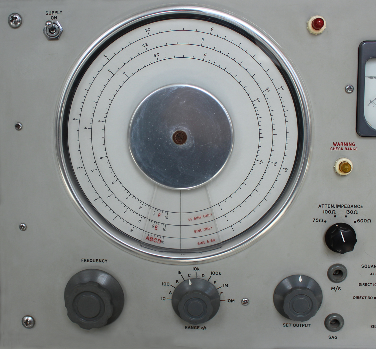
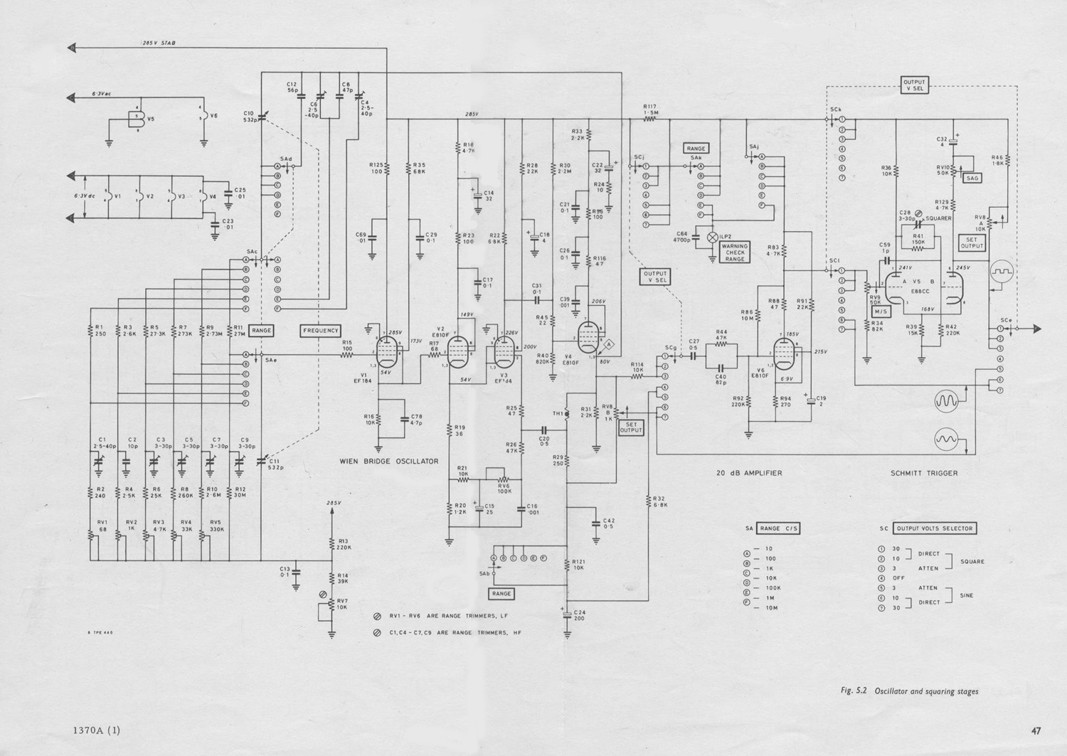
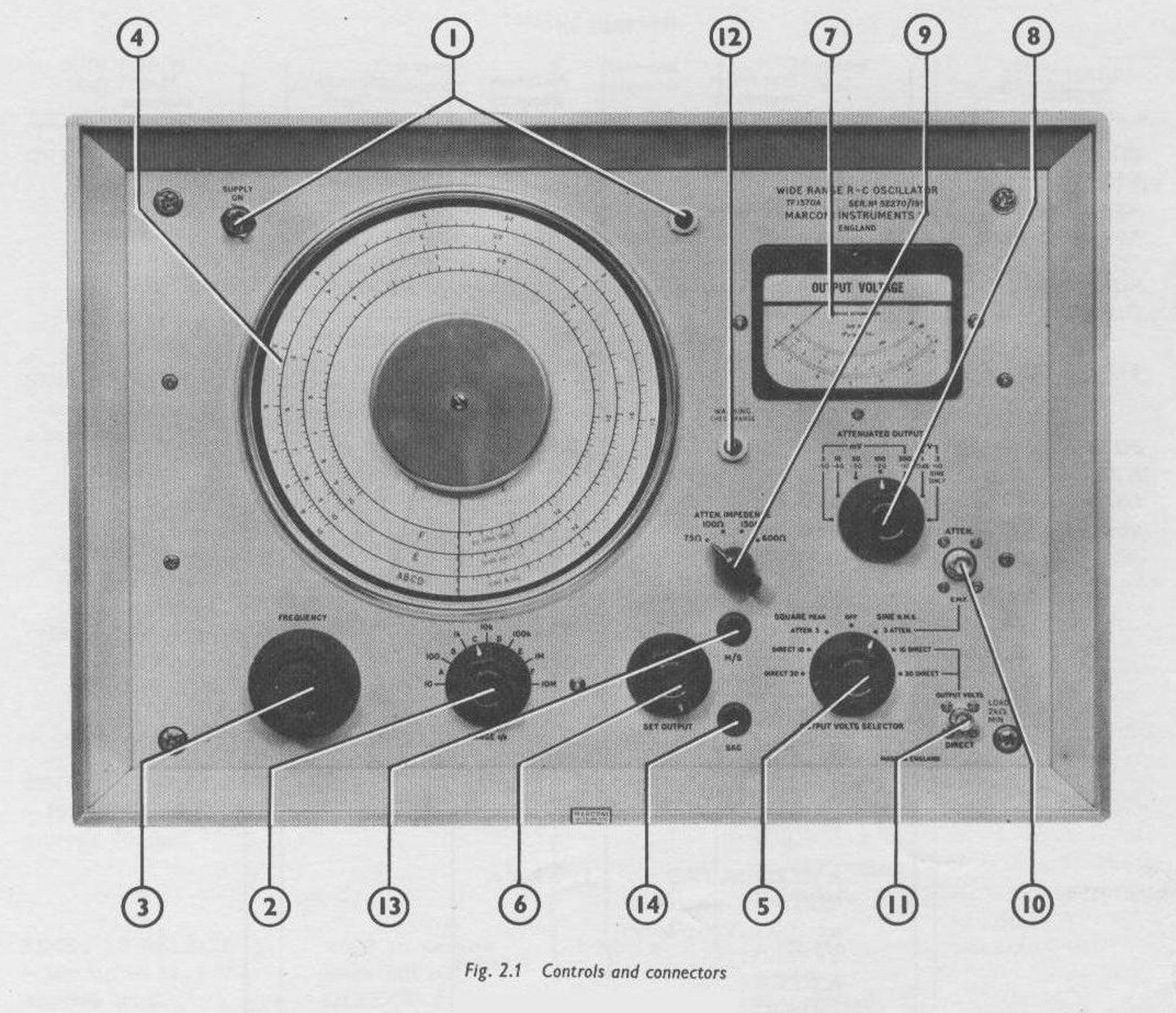
3.1 CIRCUIT ARRANGEMENT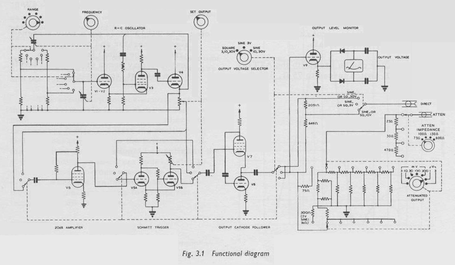 The circuits of the Wide Range R-C Oscillator are selected and combined in a number of ways by the panel controls. The Functional Diagram, Fig. 3.1 shows how the circuits are employed. The basic oscillator is a Wien bridge type utilizing variable capacitance tuning and switched resistance range selection.
For sine-wave outputs up to 3.16 V, the basic oscillator output voltage is fed direct to a cathode follower output stage: for all other sine wave outputs up to 31.6 V, the oscillator output signal is applied to the output stage via an amplifier. Square wave signals are obtained from a Schmitt circuit, which is triggered by the amplified sine wave from the basic oscillator. Square waves from the Schmitt circuit are applied to the cathode follower output stage.
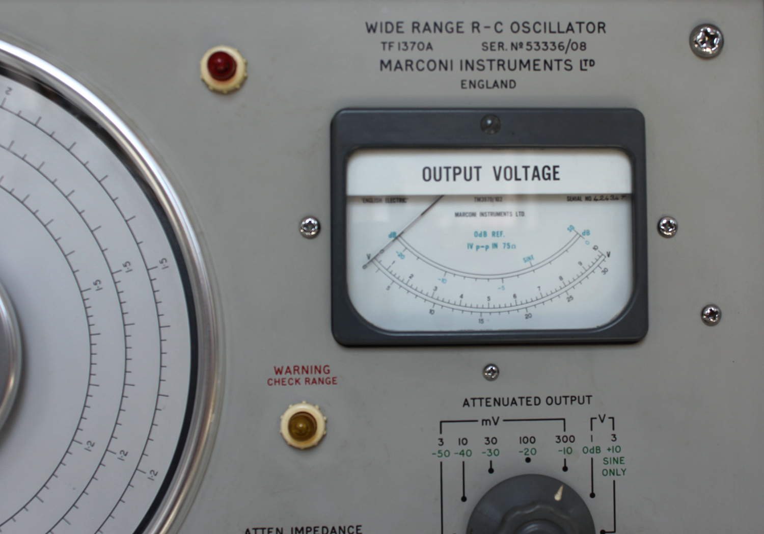
The output cathode follower feeds either the DIRECT output socket, or, via an attenuator or a 75 Ω resistor, the ATTEN output socket. The attenuator introduces 60 dB attenuation in six 10 dB steps and has a source impedance of 75 Ω. An output monitor measures the voltage at the input to the attenuator, or across a 300 Ω resistor when the attenuator is not in circuit. The front panel meter is calibrated to indicate either the source e.m.f. at the ATTEN output socket or the p. d. at the DIRECT output socket.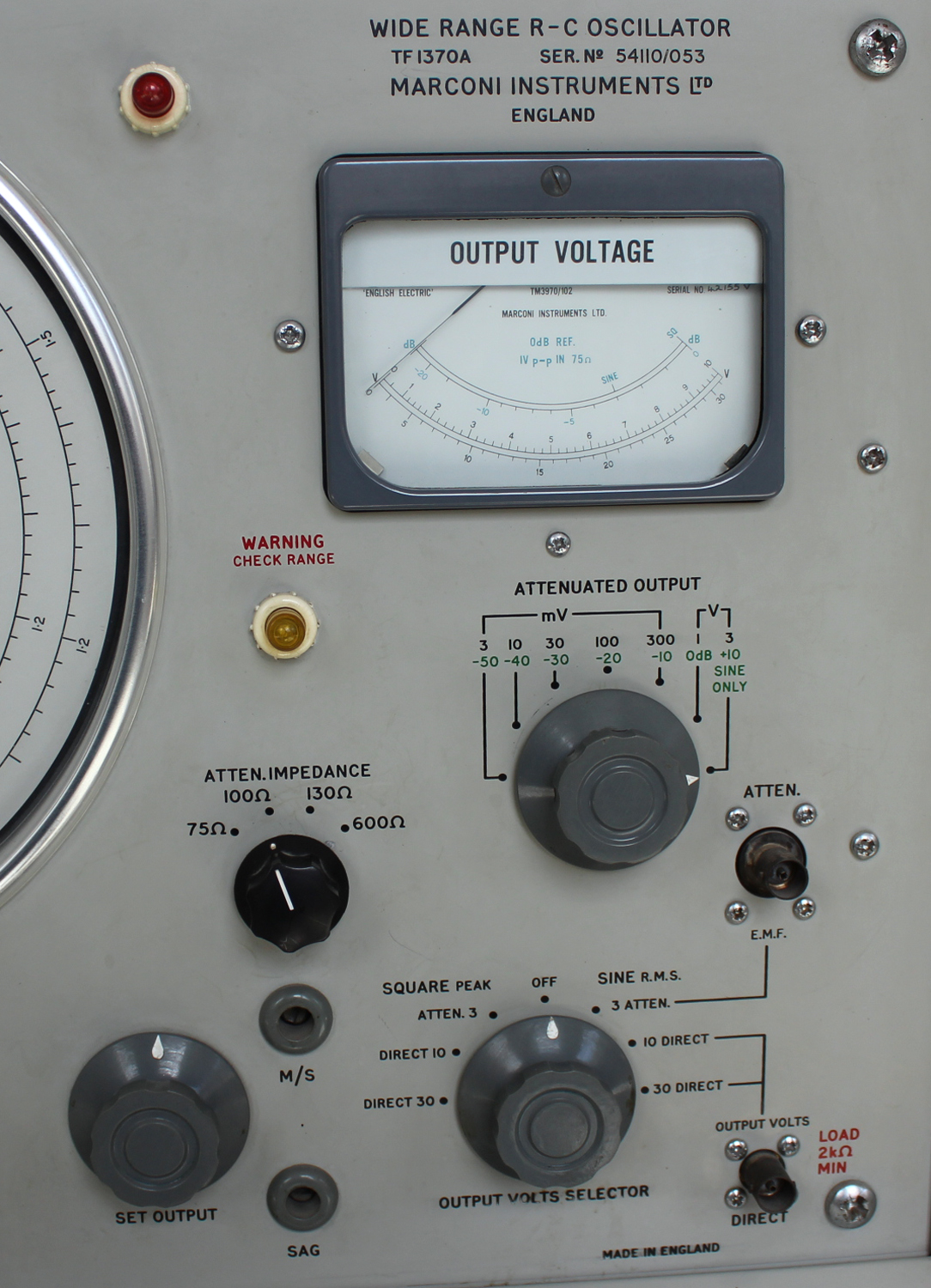 3.2 OSCILLATOR
The basic oscillator, containing valves V1 to V4, is a Wien bridge type circuit. One arm of the bridge consists of a capacitor and a resistor in series, which are connected to a second arm consisting of a capacitor and a resistor in parallel.
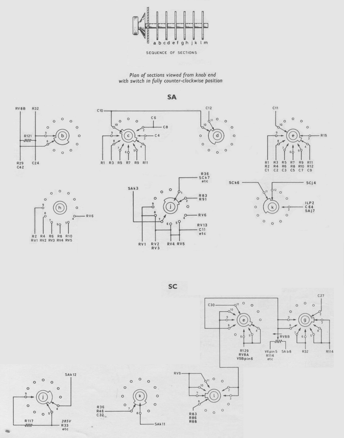
The series connected capacitor and resistor include variable capacitor C10 and one of the fixed resistors, R1, R3, R5, R7, R9, or R11; the parallel connected combination contains variable capacitor C11 and one of the resistors, R2, R4, R6, R8, R10, or R12. A particular pair of resistors is selected by the RANGE switch, SA, for each of the six frequency ranges, and the variable capacitors, C10 and C11, are ganged to provide tuning over each range. Preset variable resistors and preset variable capacitors are included in the bridge arms to enable the end frequencies of each range to be accurately set.
The second pair of arms of the bridge consist of thermistor TH1 and resistor R29.
Out-of-balance voltage developed by the bridge is applied between the control grid of V3, via capacitor C20, and the cathode of V3, via the two cathode followers V1 and V2 in cascade. The output voltage of V3 is applied – via cathode follower V4 – directly across the bridge circuit, thus forming the bridge supply voltage, which is maintained constant by thermistor TH1 controlling the degree of negative feedback.
3.3 20 dB AMPLIFIER
At all settings of the OUTPUT VOLTS SELECTOR except that giving sine waves up to 3 V, the output signal from the oscillator circuit is fed to the control grid of valve V6 from the cathode of V4 via resistor R114 for square wave operation, or via the SET OUTPUT potentiometer for sine wave operation. The amplified signal from the anode of V6 is then taken either to the Schmitt trigger (V 5A and V5B) and thence to the output cathode follower, V7, for square wave output, or direct to V7 for DIRECT sine wave output.
When the RANGE switch is turned to ranges E or F for square wave output, or range F for DIRECT sine wave output the amplifier is rendered inoperative by removing the h. t. from V6. Simultaneously a voltage is applied to the WARNING CHECK RANGE neon indicator lamp. The necessary switching is effected by switch wafers SAk, Say, SAj and SCj.
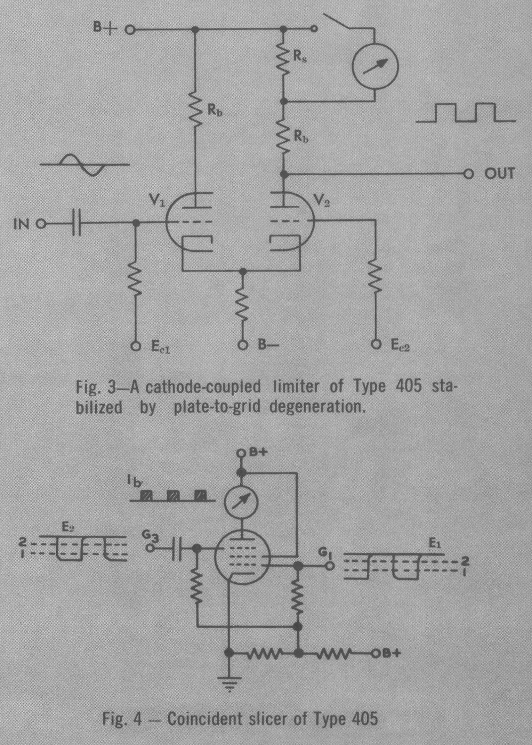
3.4 SCHMITT TRIGGER
The output voltage from the 20 dB amplifier is fed to the control grid of V5A in the Schmitt trigger circuit when the OUTPUT VOLTS SELECTOR switch, SC, is turned to the first three clockwise positions, i.e., the SQUARE, 3, 10, or 30 settings.
The Schmitt circuit, containing the two triode sections V5A and B, is triggered by the sine wave output signal from the 20 dB amplifier. One triode is held conducting while the other triode is non-conducting; the polarity of the sine wave signal applied to the control grid of the first triode section, V5A, decides which one of the two sections is conducting at any instant. To enable the switching of condition to occur at the precise base line of the sine wave input voltage, the control grid of V5A is biased by a voltage obtained from the slider of the M/S potentiometer, RV9, which is a preset control accessible at the front panel. The grid of V5A is d. c. coupled to the anode of V6; R83, the anode load of V6, forms part of the resistance chain from which the grid bias of V5A is obtained.
Preset capacitor C28, connected between the anode of V5A and the grid of V5B, is included to improve the frequency response of the coupling circuit, and is set for the best rise time. Capacitor C59, connected between the grids of the two triode sections, bucks out any curvature on the negative excursions of the square wave output signal, particularly at the higher frequencies.
The output from the Schmitt trigger circuit is fed from the anode of V5B to the grid of cathode follower V7, in the output stage, via switch SCe, capacitor C30, and resistor R49. The amplitude of the signal is controlled by varying the value of the anode load of VBB; this is achieved by variable resistor RV8A and resistor R46.
The rise time of the signal at the anode of the second triode, V5B, depends upon the value of its anode load, and reduces proportionately with the output level; so for the best performance, the amplitude of the signal should be adjusted for a front panel meter reading of about 1/3 of f.s.d.
Potentiometer RV8A is mechanically ganged to RV8B in the oscillator circuit, and the combined potentiometers function as the SET OUTPUT control.
The preset SAG control on the front panel, RV10, adjusts the flatness of the horizontal part of the output signal waveform.
This correction, mainly necessary below 100 c/s, is achieved by introducing into the waveform some curvature in opposition to the sag caused by the coupling capacitors following the Schmitt circuit. The correcting circuit consists of capacitor C32, resistor R46, a part of the SET OUTPUT control RV8A according to its setting, and variable resistor RV10. The inclusion of RV8A in the SAG control circuit ensures that the horizontal flatness of the waveform is largely independent of the SET OUTPUT control setting, particularly for outputs up to 1/3 of full-scale front-panel meter indication.
3.5 OUTPUT CATHODE FOLLOWER
The output voltage from the basic oscillator, the 20 dB amplifier, or the
Schmitt trigger circuit, is fed to the control-grid of output cathode follower V7, depending upon the setting of the OUTPUT VOLTS SELECTOR switch, SC.
The shunt-compensated cathode follower output stage contains two pentodes, V7 and V8, connected in series. The lower pentode, V8, is triode connected and forms the cathode load of the upper pentode, V7. The signal voltage developed across resistor R50 in the anode circuit of V7, is fed via capacitor C35 to the control grid of V8, thus supplementing the output signal at the cathode of V7. The output stage introduces only an extremely small amount of distortion and has an output impedance of about 15 Ω.
The signal voltage is taken from the cathode of VT and feeds the DIRECT or the ATTEN output socket via the output attenuation networks, according to the position of the OUTPUT VOLTS SELECTOR switch.
3.6 OUTPUT MONITOR
The output monitor circuit, containing meter M1 and diodes MR1 and MR2, functions as a push-pull mean—Reading rectifier circuit fed via cathode follower V9. The meter scale is calibrated in r.m.s. values for sine waves and peak readings for square waves. Resistor R81 is connected in circuit when measuring square wave voltages and is short circuited for sine wave measurements, the circuit having a. greater sensitivity to square wave inputs.
Potentiometer RV11 connected in series with the meter sets the sensitivity of the meter. Capacitors C43 and C44 provide the necessary a.c. path for the rectifying diodes, and in addition C44 prevents d.c. flowing between the positive cathode of V9 and earth via diode MR1 and the meter. Capacitor C45 is included in the circuit to reduce the d.c. leakage current in capacitor C44, which would normally affect the meter indication. C45 charges up through resistor R60 to near the potential of the cathode of V9, leaving only a. small d.c. polarizing potential across capacitors C43 and C44. Capacitors C66 and C67 function as by-pass capacitors. They prevent any r.f. currents, which may be induced in the connecting leads, from passing through the meter.
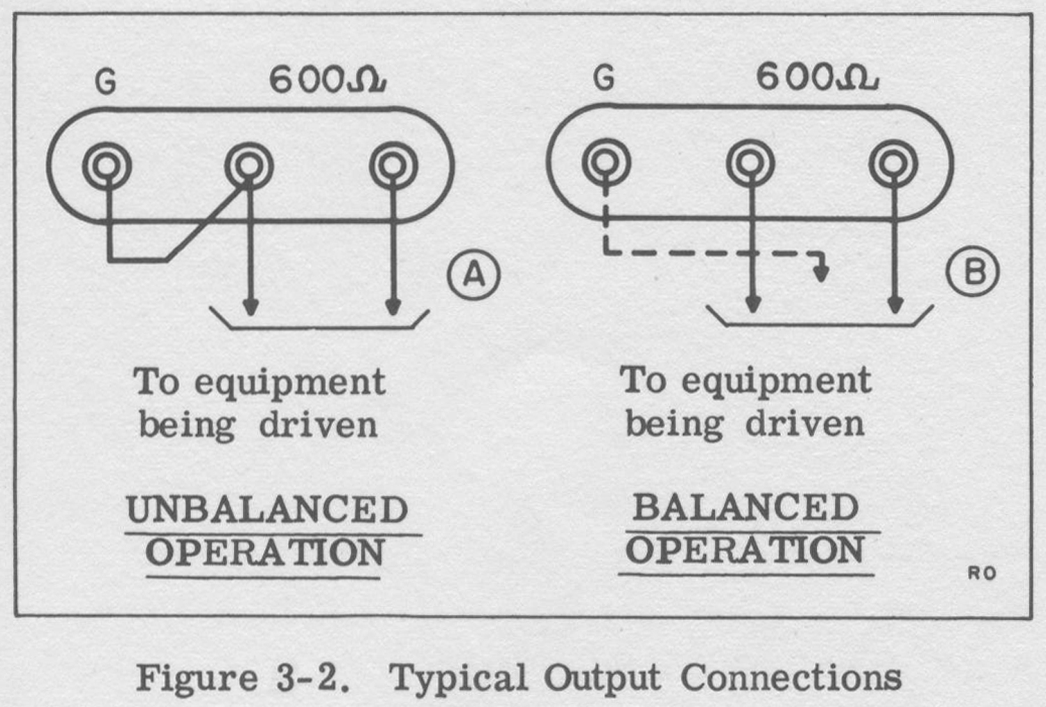
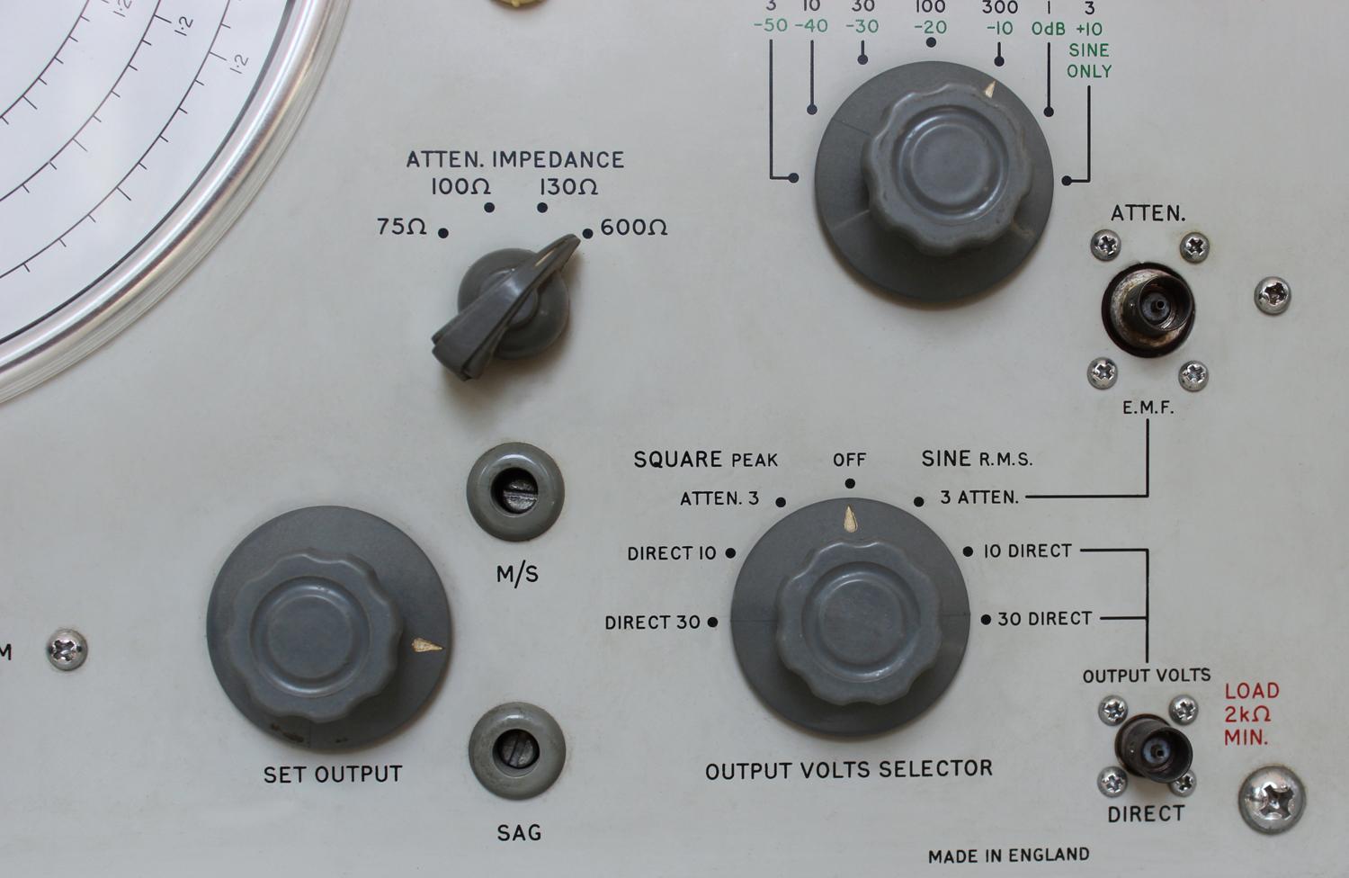
3.7 OUTPUT CONNECTIONS
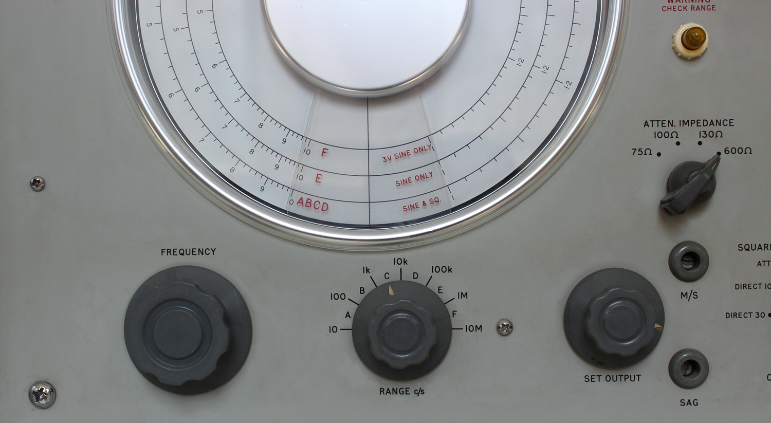
Output from the cathode follower V7 is fed to either the DIRECT or the ATTEN output socket via attenuation and impedance adjusting networks, arranged according to the position of the OUTPUT VOLTS SELECT OR switch, SC, as follows:
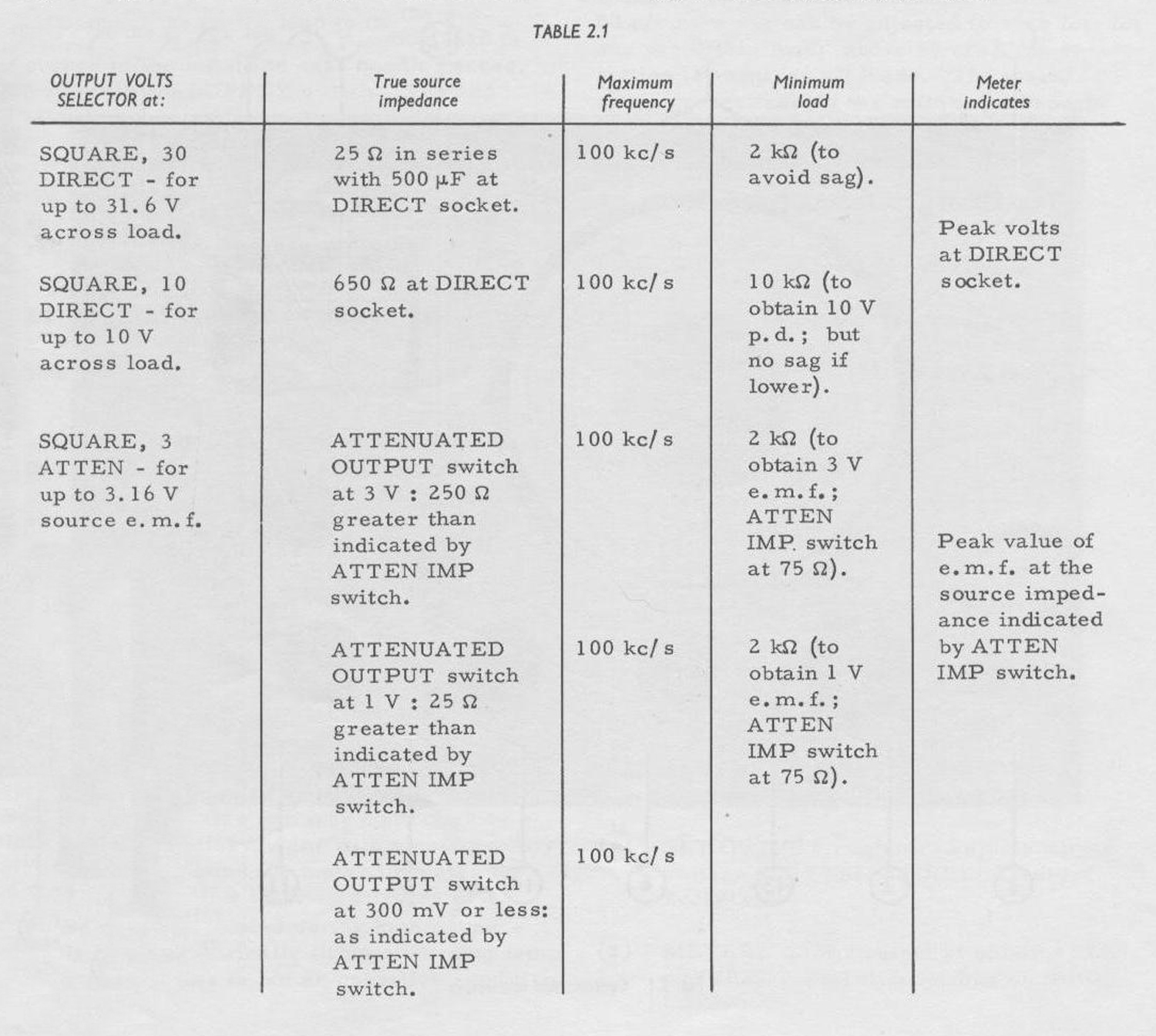
(1) SINE or SQUARE, 30 DIRECT:
Output from V7 is fed via C36 and C37, and switch SC, to the DIRECT output socket at a source impedance of 25 Ω. The output monitor measures one tenth of the output voltage, i. e. , measures the voltage appearing across the 300 Ω input impedance to the step attenuator circuit (or the 300 Ω resistor R59) that is connected in series with R64 and R65. The meter calibration on the lower scale, 0-31.6 V, indicates the actual voltage at the DIRECT output socket.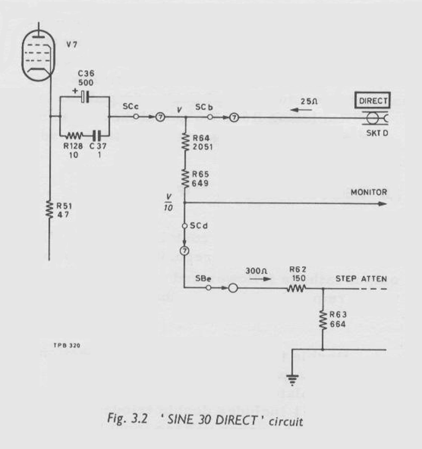
(2) SINE, or SQUARE, 10 DIRECT:
Output from V7 is fed via C36 and C37, and switch SC, to resistor R64. The signal output is taken from the junction R64/R65 and is one third of the voltage from the cathode of V7. The source impedance is 650 Ω. The output monitor measures one tenth of the voltage from V7, i. e. , measures the voltage appearing across the 300 Ω input impedance to the attenuator circuit (or the 300 Ω resistor R59) that is connected in series with R64 and R65. The meter calibration on the centre scale, 0 -10 V, indicates the actual voltage at the DIRECT output socket.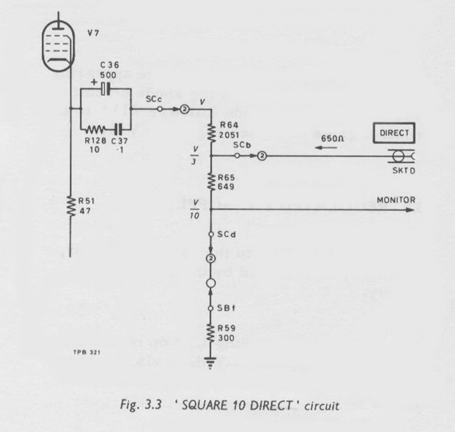 SINE, 3 ATTEN:
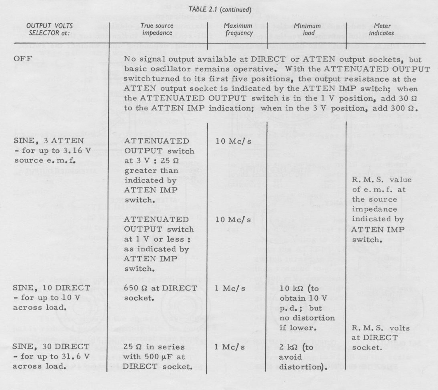
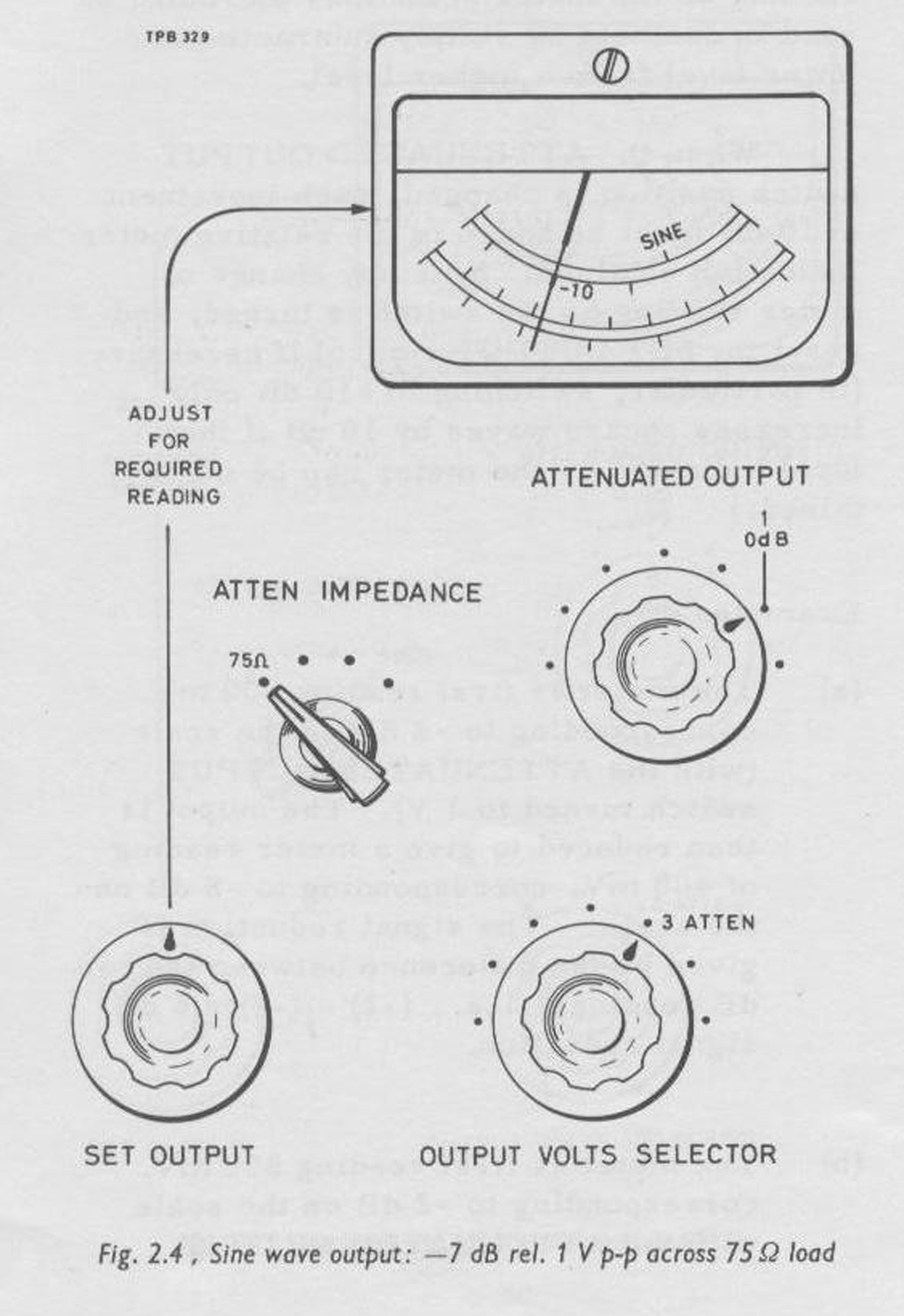
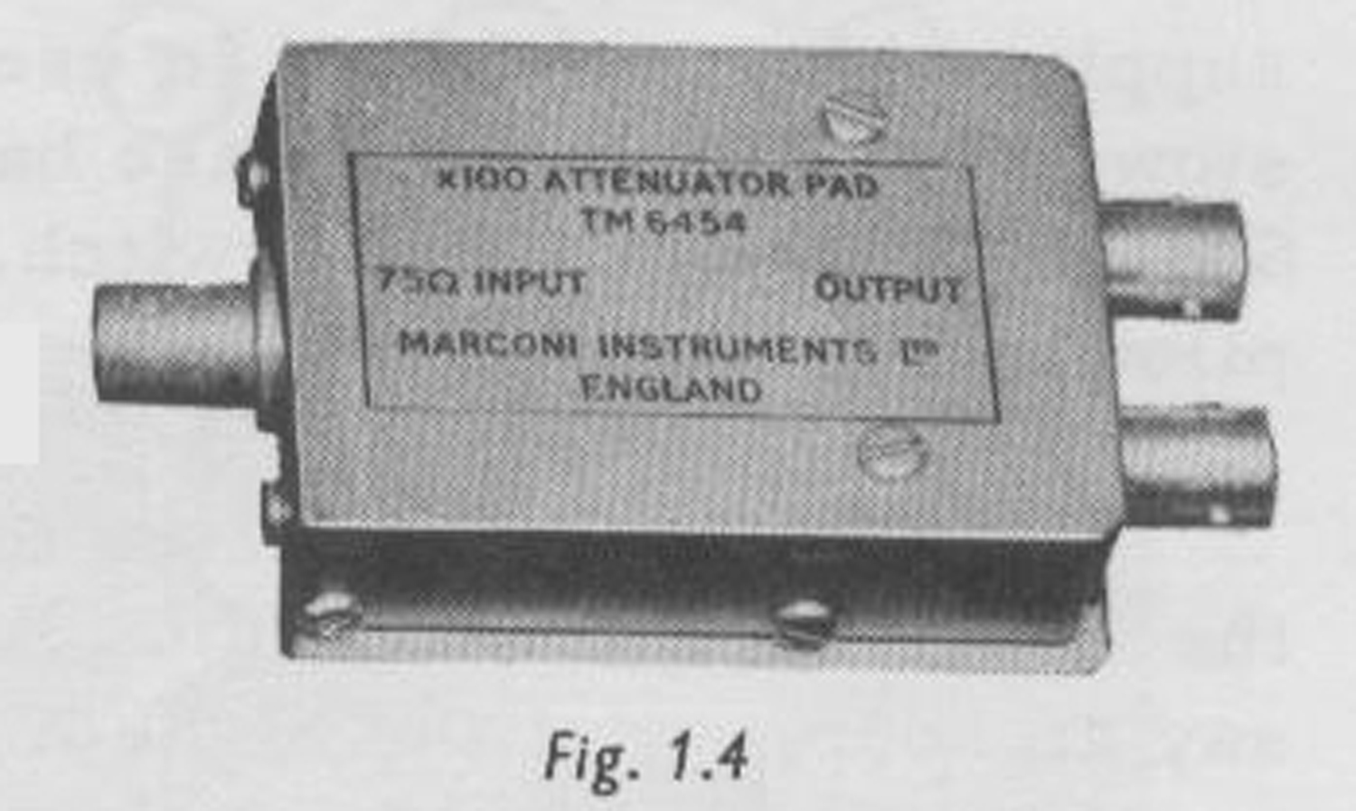
Output from V7 is applied via C36 and C37 to the step attenuator network feeding the ATTEN outlet. The attenuator network includes a chain of six 10 dB sections, which are progressively withdrawn as the ATTENUATED OUTPUT switch, SB, is turned clockwise. At the seventh position, 3 V, SB substitutes a 75 Ω series resistor, R68.
Source impedance at the ATTEN outlet is selected by the ATTEN IMPEDANCE switch SE. When this is set to 75 Ω, the source impedance is the 75 Ω output impedance presented by the stages of the step attenuator except that, if SB is set to 3 V, the 75 Ω series resistor combines with the output impedance of V7 giving a true source impedance of approximately 100 Ω at the outlet.
Turning the ATTEN IMPEDANCE switch to 100, 130 and 600 Ω adds R119, 25 Ω, R98, 30 Ω and R82, 470 Ω, cumulatively in series with the ATTEN outlet.
The output monitor measures the voltage from V7 and indicates the source e.m.f. in series with the selected source impedance. The meter scales should be read in conjunction with the setting of SB. When SB is set to 3 V, since the monitor indicates the voltage at the point where V7 feeds the 75 K2 series resistor, it therefore indicates the e.m.f. at the selected nominal source impedance, excluding the output impedance of V7.
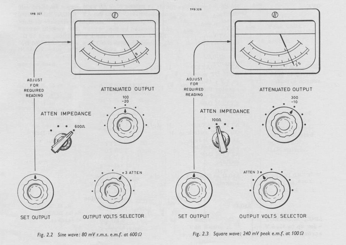
R59 ensures a. leakage path for the electrolytic capacitor C36 if a. load is not connected when SB is in the 3 V position.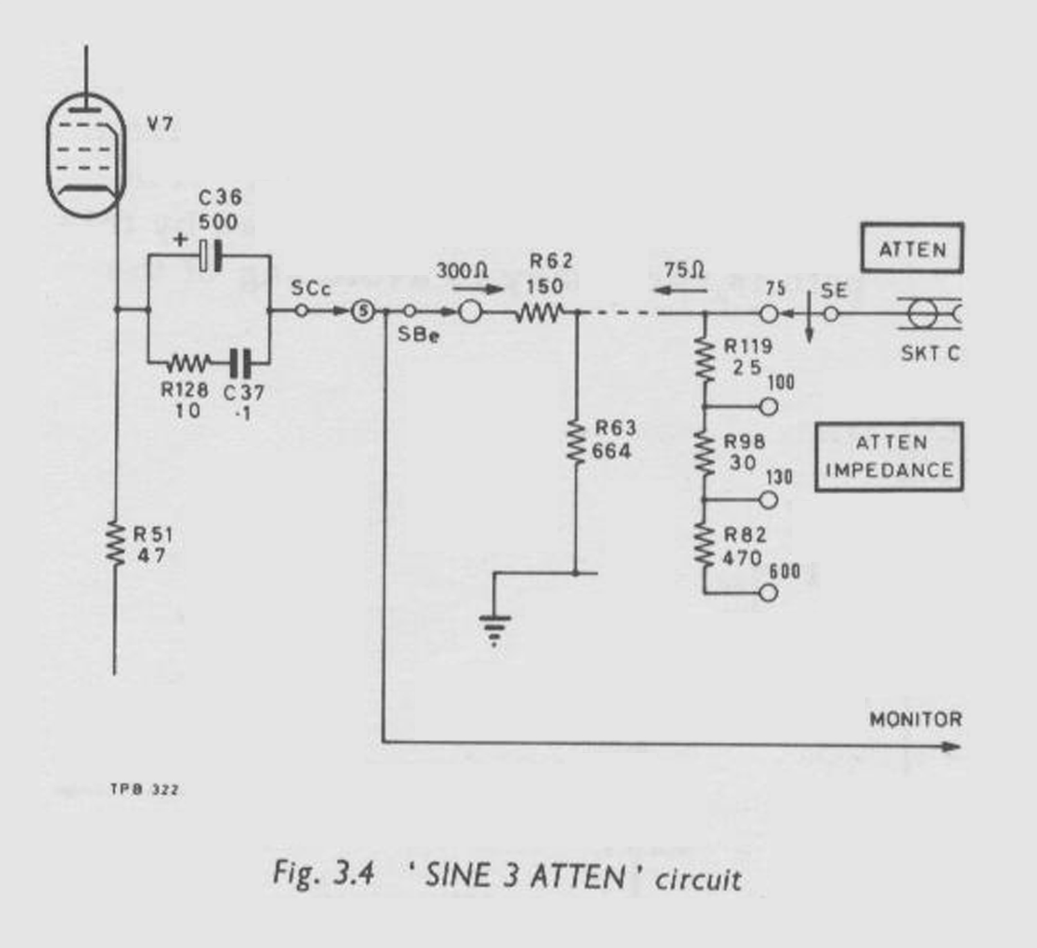 (4) SQUARE, 3 ATTEN:
The output circuit arrangement is the same as that described for SINE, 3 ATTEN, except that the step attenuator network receives its input from C36 and C37 via. R64 and R65. The long CR time constant provided by this path is necessary to avoid sag of the square wave. However, the presence of R64 and R65 has the effect of raising the true source impedance at the ATTEN outlet as the ATTENUATED OUTPUT switch, SB, is turned to positions of high output (see Table 2.1 in section 2. 6).
The output monitor measures the voltage at the 300 Ω input of the attenuator chain (or across R59) and indicates the source e.m.f. in series with the selected nominal source impedance, excluding R64, R65, and the output impedance of V7.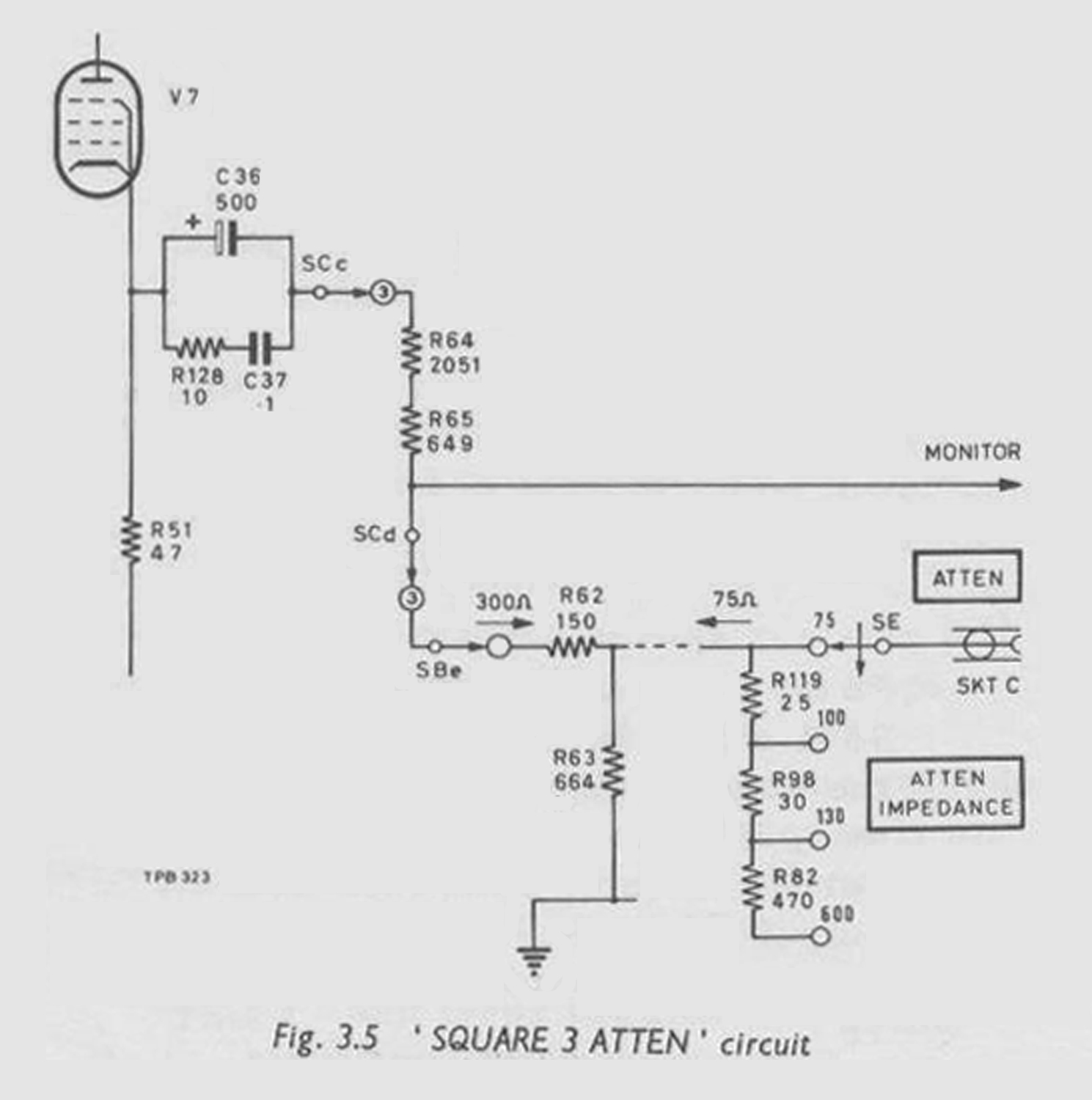 3.8 REGULATED H.T. SUPPLY
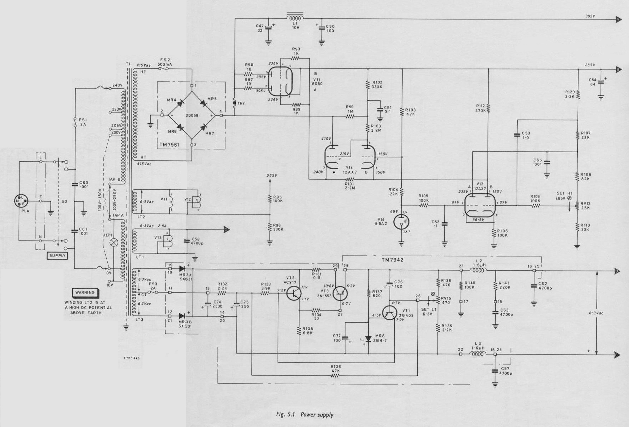
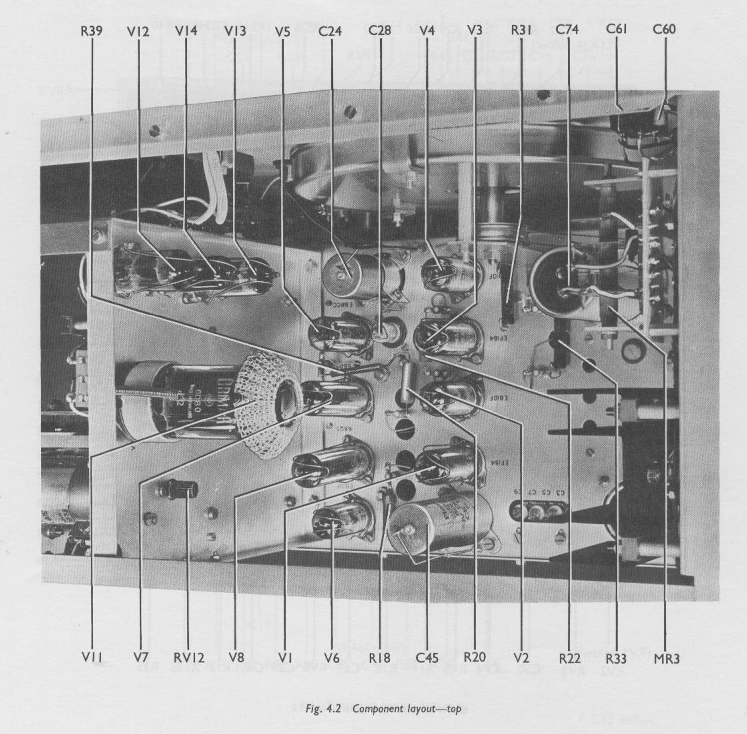
The power unit, containing valves V10 to V14, supplies an unregulated 400 V to the output cathode follower and a regulated 285 V to the remaining stages in the instrument.
Double triode V11 has its two sections connected in parallel and functions as a series regulator. The shunt amplifier that controls V11 includes double triodes V12 and V13. The error voltage input to this amplifier is the difference between (i) a fraction of the h.t. potential, obtained from the slider of the potentiometer RV12, and (ii) the reference potential developed by stabilizer V14. These two potentials are individually applied to the grids of the two cathode coupled triodes of V13. Any change of h.t. potential applied via RV12 to V13 is reinforced by the other half of V13, which draws its anode current from the resistor chain feeding RV12. The half of V13 to which RV12 is connected is coupled to the cathode of V12B in a cascade arrangement.
The amplified error voltage appearing across resistor R100 in the anode circuit of V12B is fed via cathode follower V12A to the control grids of series regulator V11. 3.9 REGULATED L.T. SUPPLY
The 1.t. d.c. to the basic oscillator, V1 to V4, is provided by the regulated 1.t. supply.
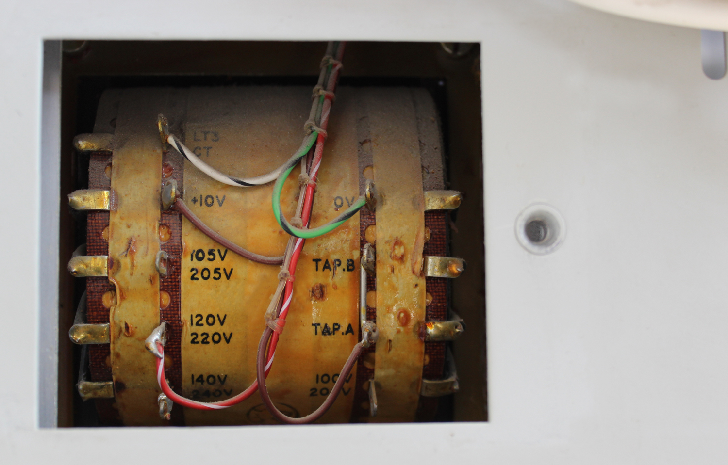
Secondary winding LT3 on mains transformer T 1 supplies 11 V d.c. via bi-phase rectifier MR3 (A and B), at nominal mains input.
Transistors VT1, VT2 and VT3 form a stabilizer circuit consisting of an amplifier, an emitter follower and a series regulator. Part of the output voltage, taken via RV15, is compared by the amplifier with a. reference voltage provided by a Zener diode, MR8. The resultant error signal is fed to the base of the series regulator, VT3, by the emitter follower, thereby controlling VT3 and keeping the output voltage constant.
Preset potentiometer RV15 is set to give an output voltage of 6.3 V.»
§§§
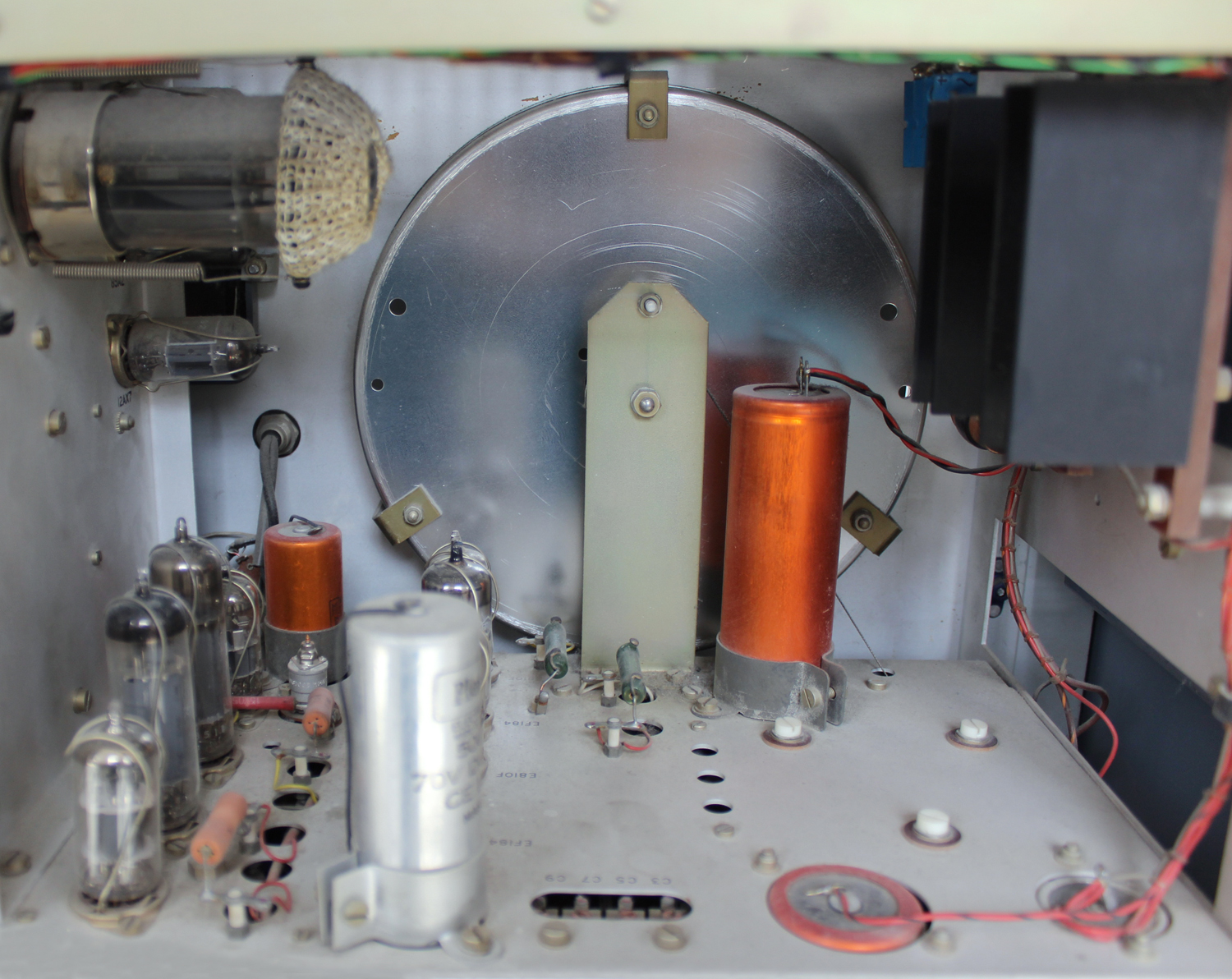
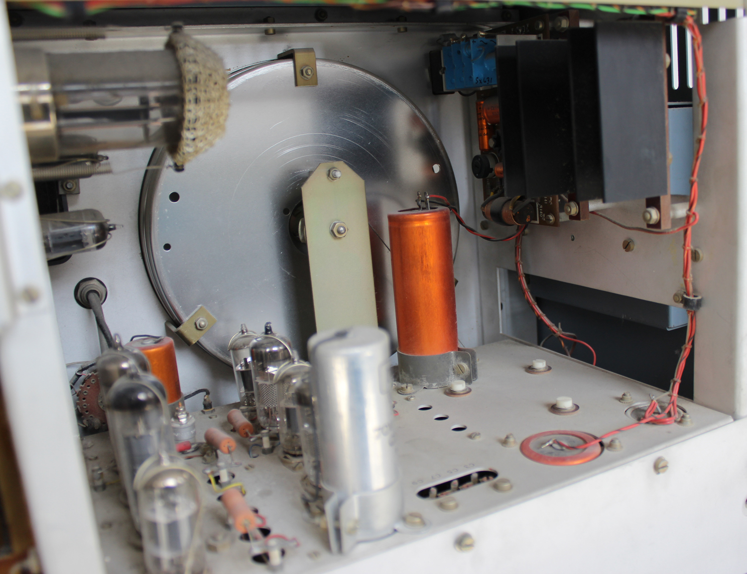
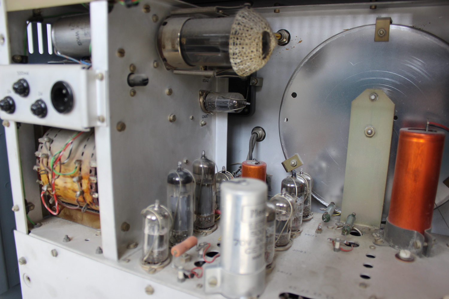
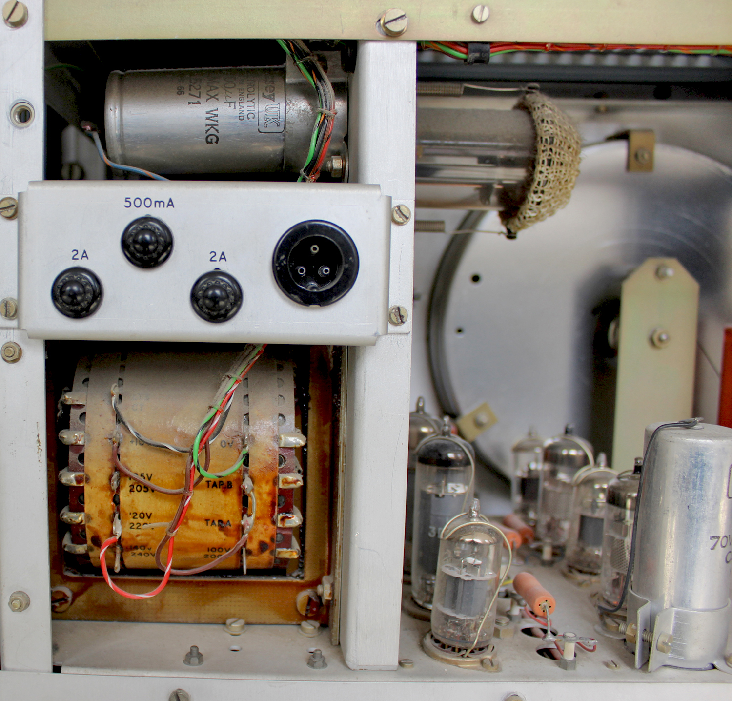
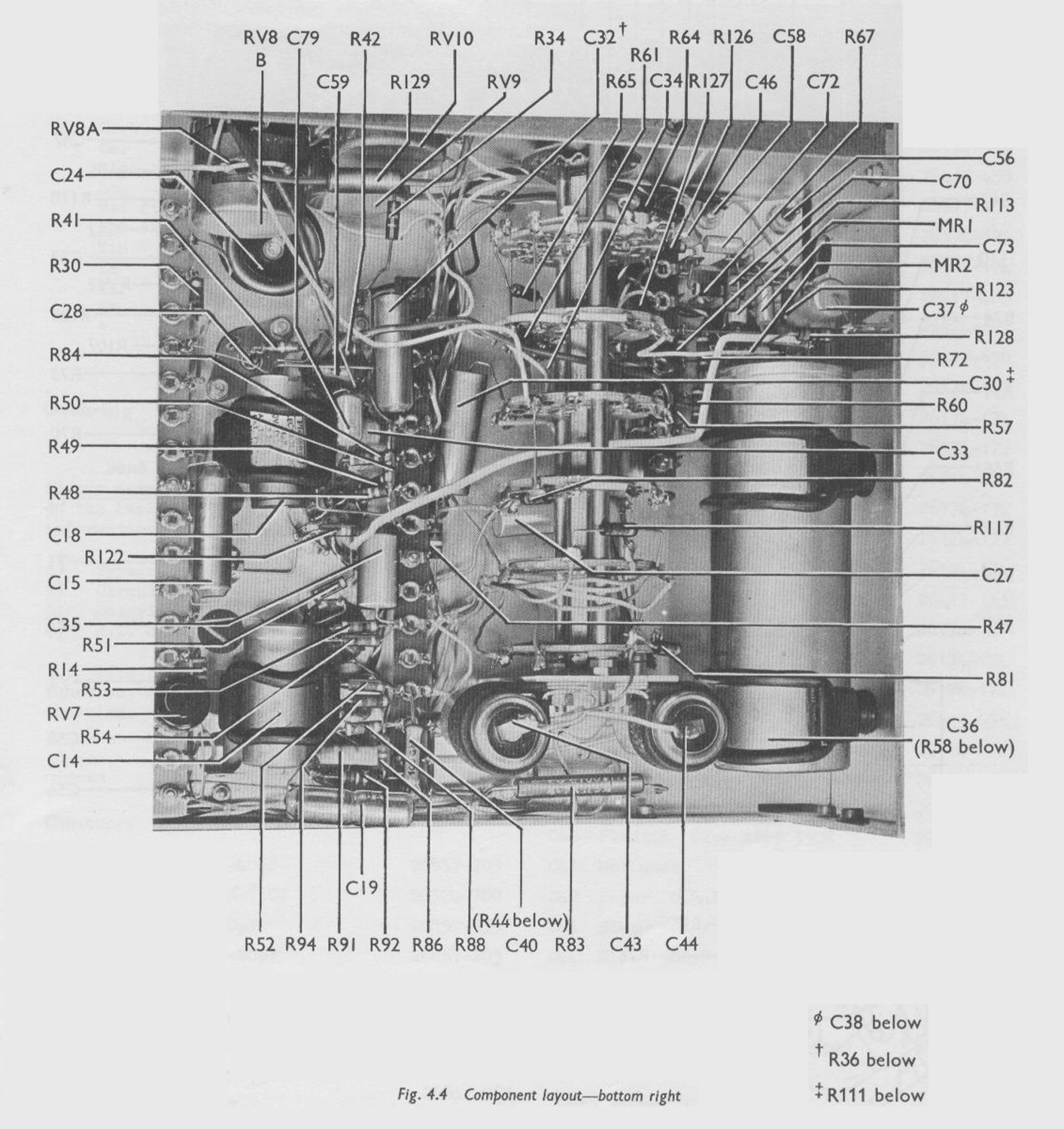
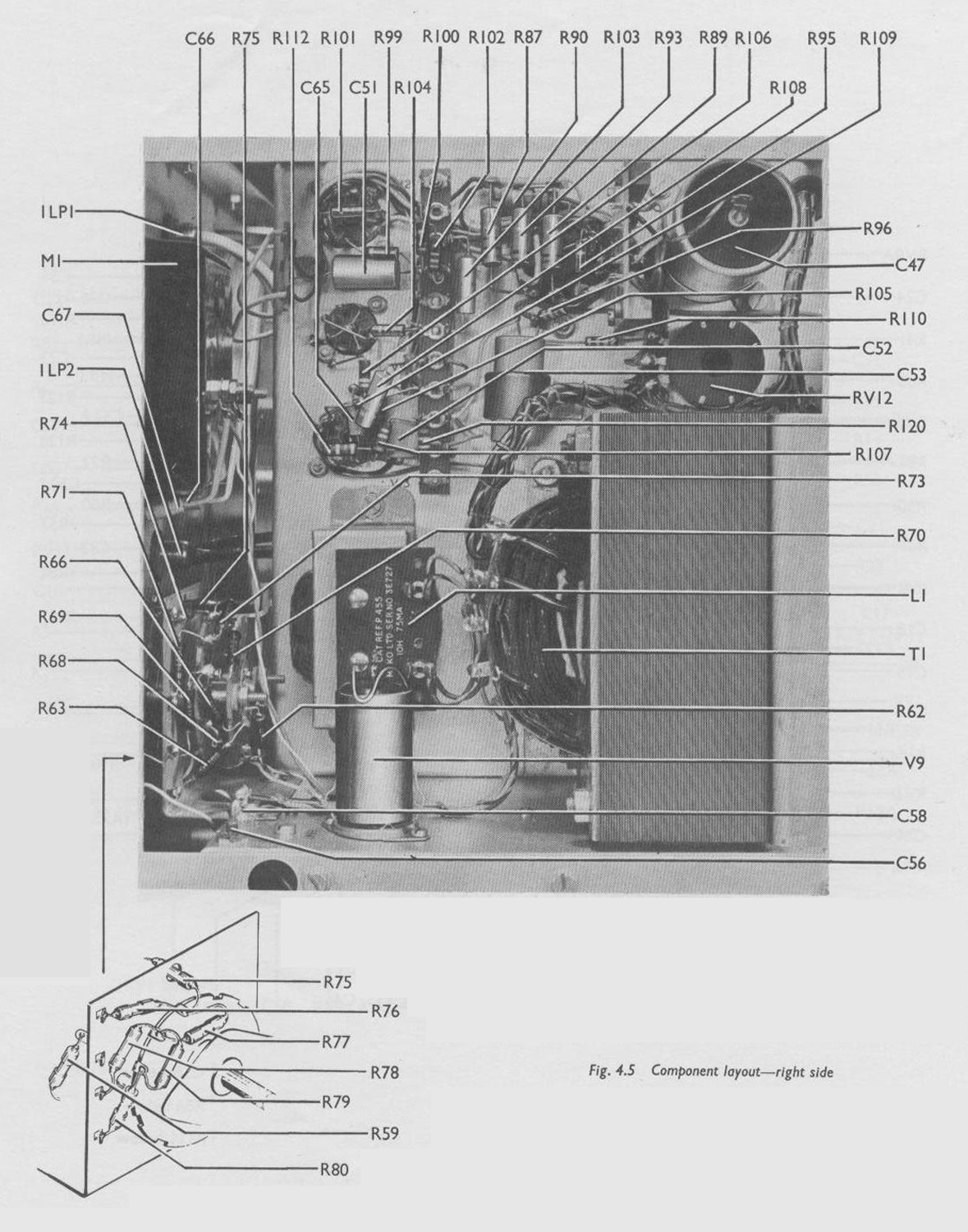
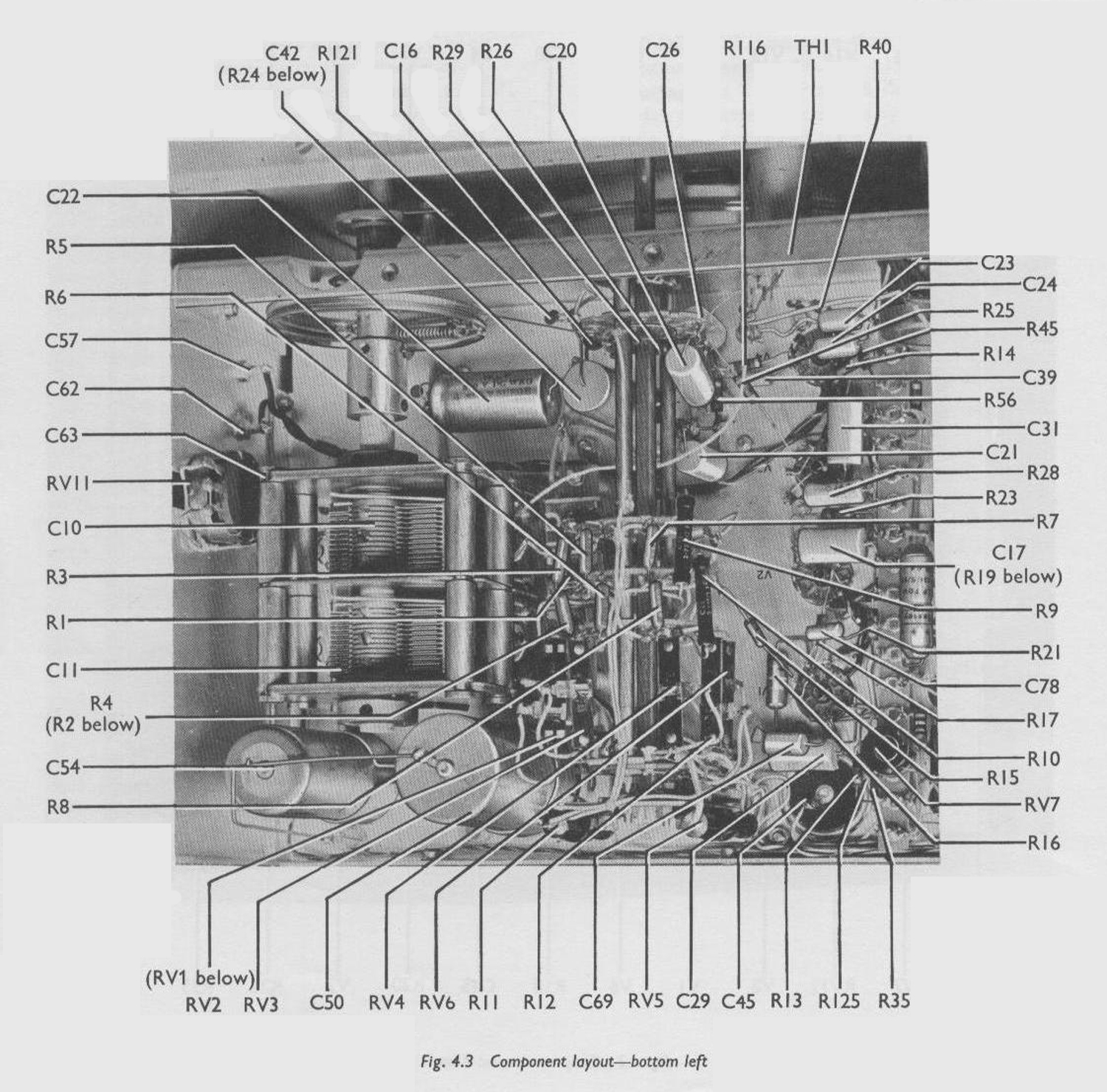
Abbiamo omesso il capitolo “Maintenance” del quale abbiamo scelto alcune figure.
Foto di Claudio Profumieri, elaborazioni e ricerche di Fabio Panfili. Testo a cura di Fabio Panfili.
Per ingrandire le immagini cliccare su di esse col tasto destro del mouse e scegliere tra le opzioni.


 «1 GENERAL INFORMATION
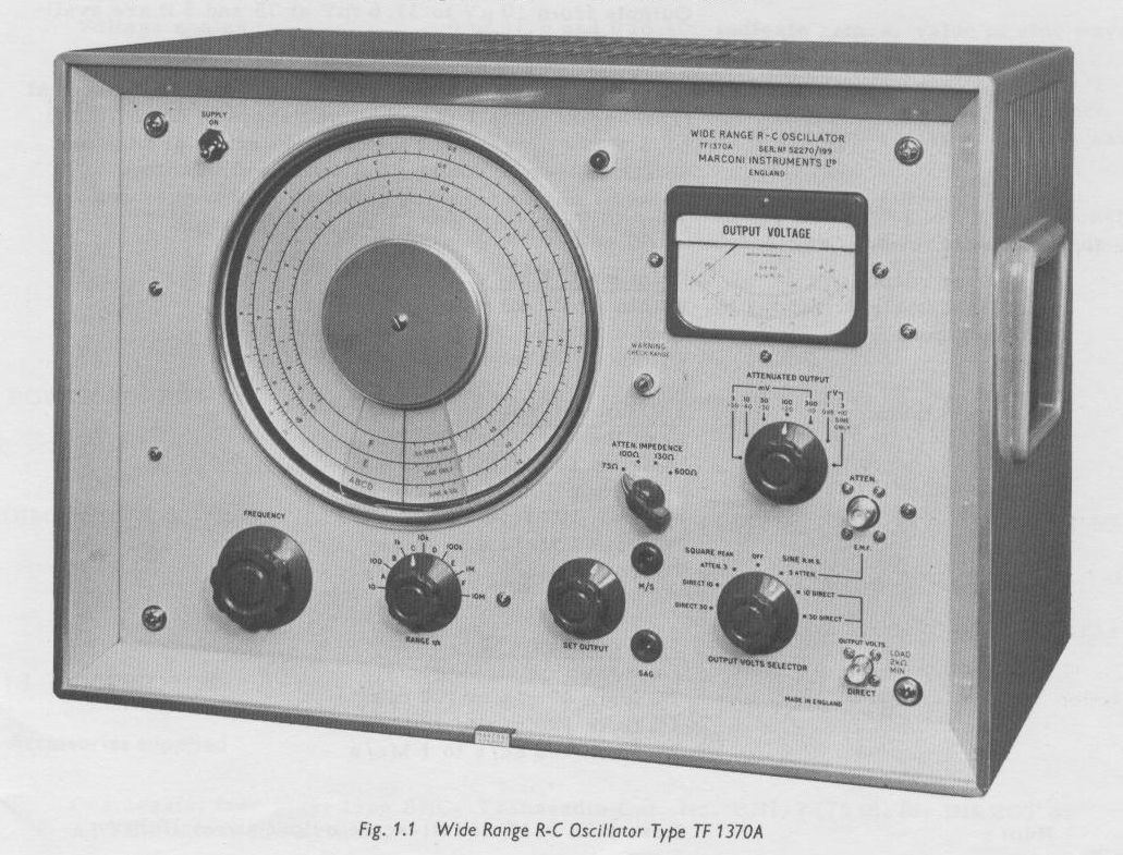
 SECTION I
 SECTION III