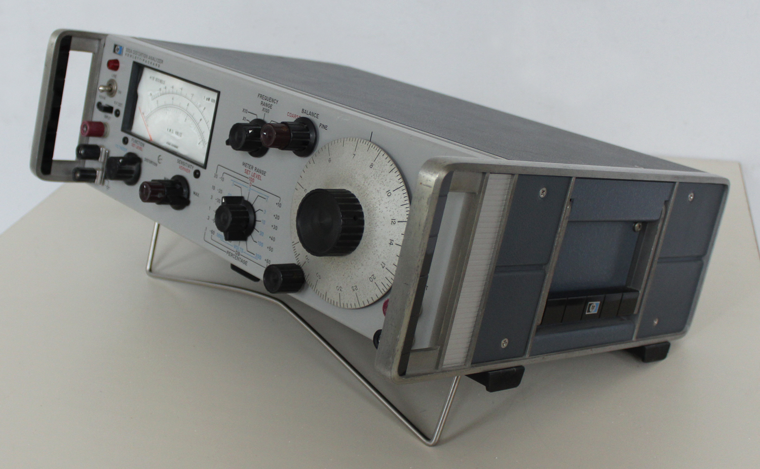
 Distortion Analyzer Hewlett Packard 332A matr. N° 930 – 96620. Terza parte.
Nell’inventario particolare del Laboratorio di Elettronica al n° D 4826, in data ottobre 1970, si legge: “Distortion Analyzer S/N 620 mod. 332A”.
Nell’HEWLETT·PACKARD Journal VOL. 17 NO. 8 APRIL 1966 vi è addirittura la presentazione del modello 334A che nell’amplificatore di eliminazione della tensione a frequenza fondamentale (rejection) ha il ponte di Wien, come questo mod. 332A e come l’esemplare -hp- 330B che si può vedere in questo sito nella sezione Radiotecnica.
Il testo è stato tratto dal manuale di istruzioni OPERATING AND SERVICE MANUAL DISTORTION ANALYZER 331A/332A HEWLETT hp PACKARD Printed JUNE 1969, conservato presso la Sezione Elettronica.
Istruzioni quasi identiche si possono trovare ad esempio all’indirizzo: https://www.artisantg.com/info/ATGx6v9r.pdF
Il testo prosegue dalla seconda parte.
§§§
« SECTION IV
THEORY OF OPERATION
4-I. OVERALL DESCRIPTION.
4-2. Models 331A and 332A Distortion Analyzers include an impedance converter circuit, a rejection amplifier, a metering circuit, and a power supply circuit. In addition to these four circuits, the Model 332A contains an AM detector circuit. A block diagram of the instrument is shown in Figure 4-1.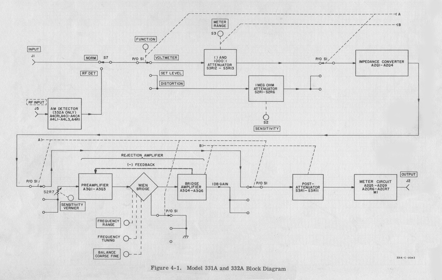 The impedance converter provides a low noise input circuit with a high source impedance independent of signal impedance placed at the input terminals. The rejection amplifier rejects the fundamental frequency of an input signal and passes the remaining frequency components on to the metering circuit for measuring distortion. The metering circuit provides visual indications of distortion and voltage levels on the front panel meter M1. The AM detector circuit (Model 332A only) detects the modulating signal from the RF carrier and filters any RF components from the modulating signal before it is applied to the impedance converter circuit.
4-3. BLOCK DIAGRAM DESCRIPTION.
(Refer to Figure 4-1.)
4-4. DISTORTION MEASURING OPERATION.
4-5. In the distortion measuring mode of operation, the input signal is applied to the impedance converter circuit (Assembly A2) through the FUNCTION selector, S1, and the one megohm attenuator. The attenuator is a voltage divider network which provides 50 dB attenuation in 10 dB steps. The desired level of attenuation is selected by the SENSITIVITY selector , S2. The impedance converter circuit provides an impedance conversion and unity gain between the instrument input terminals and the input of the rejection amplifier.
4-6. The rejection amplifier consists of a preamplifier, a Wien bridge, and a bridge amplifier circuit. The SENSITIVITY VERNIER control, at the input of the preamplifier circuit, provides a set level signal to obtain full scale readings on meter M1 for any input voltage level. With the FUNCTION selector in the SET LEVEL position , a ground is applied to the Wien bridge circuit to allow a signal reference level to be set up on the meter M1 in the metering circuit.
With the FUNCTION selector in the DISTORTION position, the Wien bridge is used as an interstage coupling network between the preamplifier and bridge amplifier circuits. The Wien bridge is tuned and balanced to reject the fundamental frequency of the applied input signal. The remaining frequency components are passed on to the bridge amplifier circuit and are measured as distortion by the metering circuit. Negative feedback from the bridge amplifier to the preamplifier narrows the rejection response of the Wien bridge circuit.
4-7. The output of the rejection amplifier (1 dB gain) is applied to the metering circuit through the post-attenuator. The post-attenuator is used to limit the input signal level applied to the metering circuit to 1 mV for full scale deflection. The metering circuit sensitivity is increased to 300 μV for full scale deflection on the 0.0003 V range. The metering circuit provides a visual indication of the distortion level in the input signal. In addition to the visual indication provided by the meter M1, the OUTPUT terminals provide a means of monitoring the distortion with an oscilloscope , a true rms voltmeter, or a wave analyzer.
4 -8 . DISTORTION MEASUREMENT IN AM CARRIERS
4-9. The Model 332A Distortion Analyzer contains an AM detector circuit for measuring envelope distortion in AM carriers. The input signal is applied to the input of the AM detector circuit where the modulating signal is recovered from the RF carrier. The signal is then applied to the impedance converter circuit through the one megohm attenuator. The signal then goes through the same circuits previously described in the distortion measuring operation.
4-10. VOLTMETER OPERATION.
4-11. In the voltmeter mode of operation, the input signal is applied to the impedance converter circuit through the 1:1 and 1000:1 attenuator. The 1:1 attenuation ratio is used in the 0.0003 to 0. 3 VOLTS positions of the METER RANGE switch S3, and the 1000:1 attenuation ratio is used in the 1 to 300 VOLTS positions. With the FUNCTION selector in the VOLTMETER position, the output of the impedance converter bypasses the rejection amplifier and is applied to the metering circuit through the post-attenuator and METER RANGE selector. In the voltmeter mode, metering circuit sensitivity is increased from 1 mV for full scale deflection to 300 μV on the 0.0003 V range, the same as it was in the distortion mode of operation. The function of the post-attenuator and metering circuit is the same for the voltmeter mode as for the distortion mode.
4-12. DETAILED CIRCUIT DESCRIPTION.
4-13. IMPEDANCE CONVERTER CIRCUIT.
(Refer to Figure 7-1.)
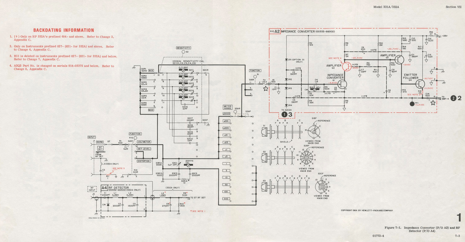
4-14. The input signal to the distortion analyzer is applied to the impedance converter circuit through the 1:1 and 1000:1 attenuator, S3R12, in the voltmeter mode of operation and through the one megohm attenuator S2R1 through S2R6 in the distortion mode of operation. Capacitive dividers act in conjunction with the attenuators to keep the frequency response flat.
The impedance converter is a low distortion, high input impedance amplifier with gain independent of the source impedance placed at the INPUT terminals.
4-15. Instrument induced distortion of the signal being measured is prevented by keeping the input impedance and the gain of the impedance converter linear. The input impedance is made linear by “boot strapping” the protection diodes A2CR2 and A2CR3 and the gate to drain capacitance of A2Q1 with local positive feedback. By keeping the input impedance linear, signals having a high source impedance can be measured accurately and the SENSITIVITY selector S2 can be used in the high impedance positions without distorting the input signal. In addition to having a high input impedance, the impedance converter serves as a linear amplifier. The open loop gain of the circuit is increased by “boot strapping” the collector load impedances of A2Q2 and A2Q3 with local positive feedback. Overall negative feedback from the emitter circuit of A2Q4 to the source of A2Q1 results in unity
gain from the impedance converter circuit and keeps the distortion generated by the circuit well within the specifications listed in Table 1-1.
4 -16. The bias points of the transistors in the impedance converter circuit have been selected for optimum distortion performance. The voltage at A2TP1 is set for optimum distortion performance for each individual instrument and should not be changed from the set value unless the field effect transistor A2Q1 is replaced. The field effect transistor used in the impedance converter provides extremely low noise performance independent of the signal source impedance, and aids in producing the high impedance input to the impedance converter circuit.
4-17. REJECTION AMPLIFIER CIRCUIT.
(Refer to Figure 7-2.)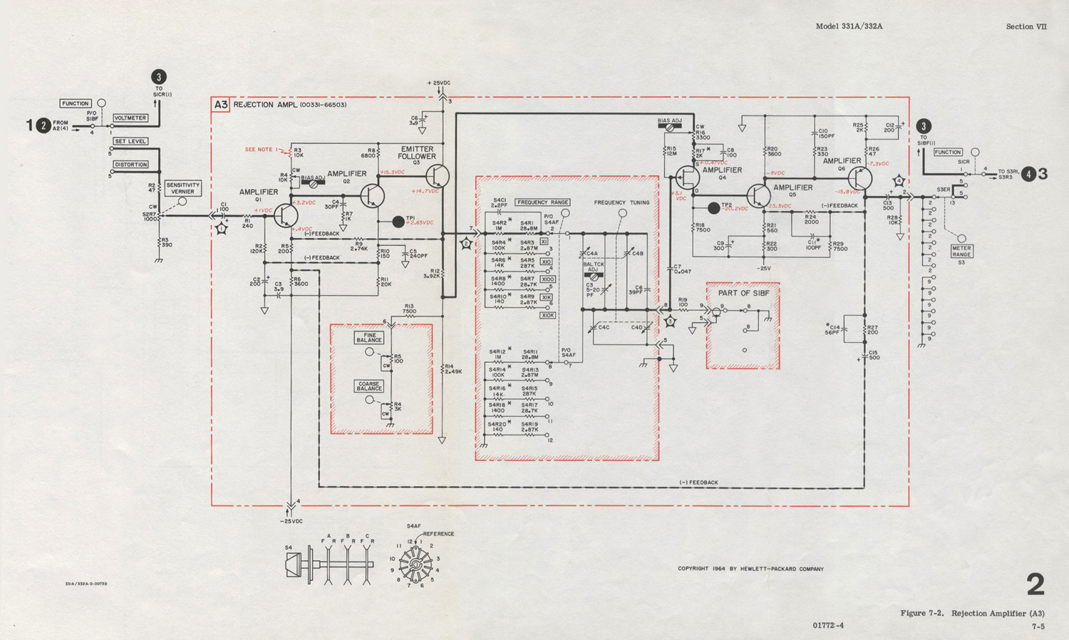 4-18. The rejection amplifier circuit consists of the preamplifier, A3Q1 through A3Q3, the Wien bridge circuit, and the bridge amplifier, A3Q4 through A3Q6. A simplified block diagram of the rejection amplifier with the typical frequency rejection characteristic is shown in Figure 4-2.
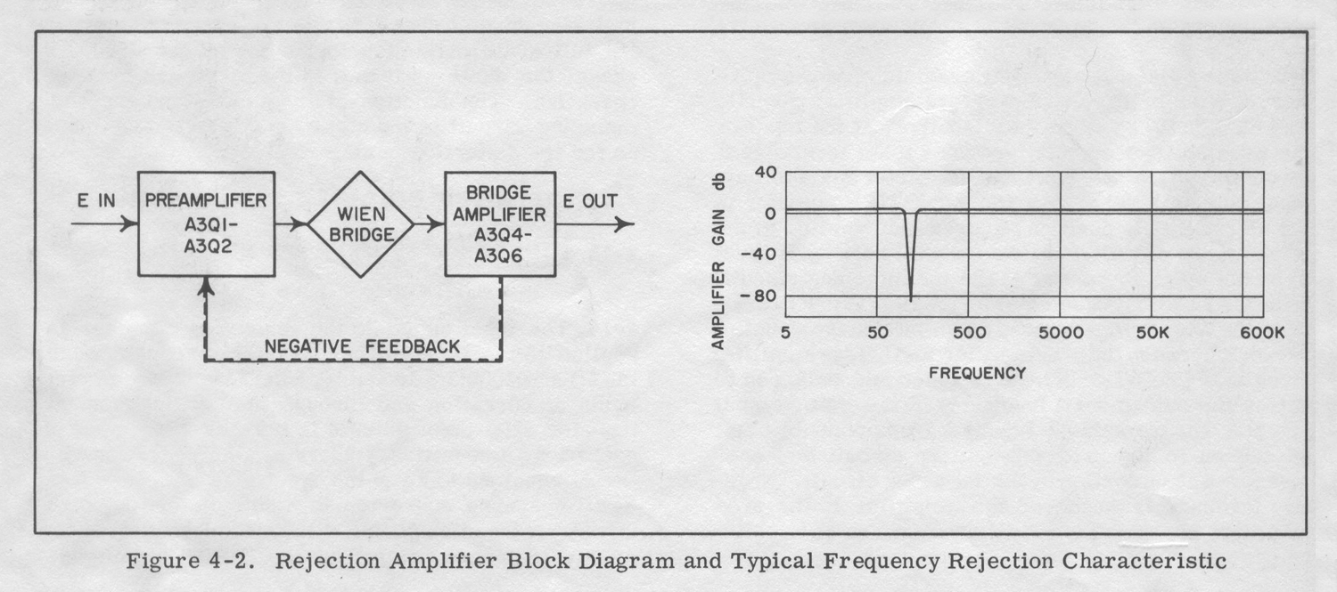 4-19. PREAMPLIFIER CIRCUIT.
4-20. The signal from the impedance converter circuit is applied to the preamplifier circuit which is operational in the SET LEVEL and DISTORTION modes of operation. Negative feedback from the junction of A3R1O and A3R11 is applied to the junction of A3R2 and A3C2 to establish the operating point for A3Q1. Negative feedback from the emitter of A3Q3 is applied to the emitter of A3Q1 to stabilize the whole preamplifier circuit. The preamplifier circuit, like the impedance converter circuit, is designed for high open loop gain to insure maximum distortion performance.
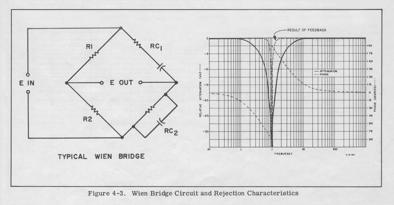
4-21. WIEN BRIDGE CIRCUIT.
4-22. The Wien bridge circuits used, in the distortion mode of operation, as a rejection filter for the fundamental frequency of the input signal. With the FUNCTION selector S1 in the DISTORTION position, the Wien bridge is connected as an interstage coupling network between the preamplifier circuit and the bridge amplifier circuit.
4-23. The bridge is tuned to the fundamental frequency of the input signal by varying the frequency tuning capacitors, C4A through C4D, after the FREQUENCY RANGE selector S4 is set for the applicable frequency range. The bridge circuit is brought into balance by adjusting the COARSE BALANCE control R4 and the FINE BALANCE control R5. When the bridge circuit is tuned and balanced, the voltage and phase of the fundamental, which appears at junction of the series reactive arm (S4R1-S4R1O and C4A/B) and the shunt reactive arm (S4R11-S4R2O and C4C/D) , is the same as at- the midpoint of the resistive branch (A3R12 and A3R14). When these two voltages are equal and are in phase, no output signal will appear at the drain of the field effect transistor A3Q4. For frequencies other than the fundamental, the reactive branch of the Wien bridge offers various degrees of attenuation and phase shift. The difference voltage between the reactive branch and resistive branch is amplified by A3Q4. Figure 4-3 illustrates a typical Wien bridge circuit and the rejection characteristic for this circuit. The Wien bridge circuit is designed to cover a continuous frequency range of 12 to 1 to insure an overlap of the coarse tuning range. Coarse tuning ranges are selected by the FREQUENCY RANGE selector S4 which changes the bridge circuit constants in five decade steps.
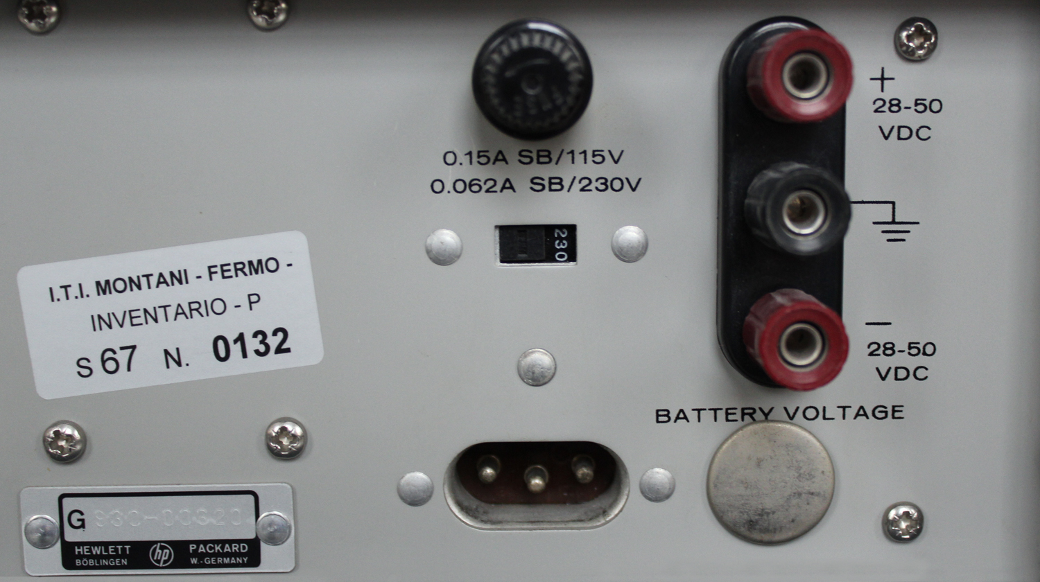
4 -24. When the FUNCTION selector is set to the VOLTMETER or SET LEVEL position, the junction of the series and shunt reactive arm of the Wien bridge is connected to circuit ground through SIBF, which disables the frequency rejection characteristic of the bridge circuit. With the bridge circuit disabled, the rejection amplifier circuit provides one dB of gain for the fundamental frequency, the harmonics, and for the residuals to establish the set level reference in the SET LEVEL mode of operation.
4-25. BRIDGE AMPLIFIER CIRCUIT.
4-26. The bridge amplifier circuit consists of three stages of amplification, A3Q4 through A3Q6. The first stage of amplification, A3Q4, is a field effect transistor which amplifies the difference signal between the gate and the source. The field effect transistor is selected for maximum noise performance with the high impedances of the Wien bridge circuit. The signal from the drain is applied to the two stage feedback amplifier A3Q5 and A3Q6. The bias potential at A3TP2 is set for maximum distortion performance for each individual instrument and should not be changed from the set value unless the field effect transistor A3Q4 is replaced.
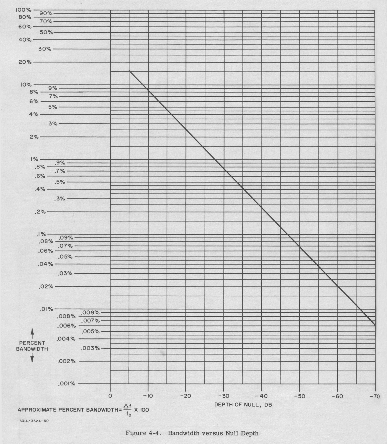
4-27. The output of A3Q6 is coupled to the meter circuit through the post attenuator S3R1 through S3R11. Negative feedback from the output of the bridge amplifier is applied to the preamplifier circuit to narrow the frequency rejection characteristic. It can be noted from the rejection characteristic (refer to Figure 4-3) for the bridge that the rejection of harmonic voltages is not constant. Typically the second harmonic is attenuated several dB more than the third harmonic, and the third more than the fourth. The result of the negative feedback is illustrated by the, rejection characteristic shown in dashed lines on the amplitude and phase characteristic of Figure 4-3. Refer to Figure 4-4, Bandwidth versus Null Depth for further detail on the rejection characteristic.
4-23. METER CIRCUIT.
(Refer to Figure 7-3.)
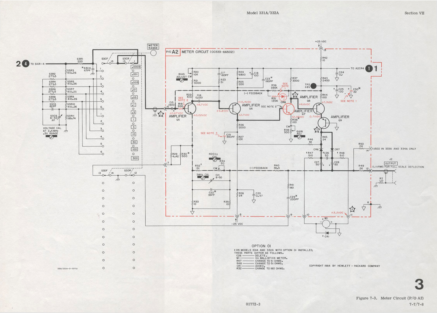
4-29 . The meter circuit consists of the post attenuator, the meter amplifier circuit, and the meter rectifier circuit.
4-30. POST ATTENUATOR.
4-31. The post attenuator, S3R1 through S3R11, is a series of resistor networks which provide attenuation of input signals in 10 dB steps. The attenuator is used in conjunction with either the input sensitivity attenuator or the 1000:1 attenuator to limit the signal level to the meter amplifier to 1 mV for full scale deflection on all ranges from 1 mV to 300 V full scale. The meter circuit sensitivity is increased to 300 μV for full scale deflection on the 0.0003 V range by switching resistors A2R29 and A2R30 into the calibration network. Resistor A2R41 and capacitor A2C29 are also switched into the calibration network on the 0.0003 V range to extend the passband of the amplifier.
4-32. METER AMPLIFIER CIRCUIT.
4-33. The meter amplifier circuit consists of five stages of amplification, A2Q5 through A2Q9, which develop the current for full scale meter deflection. Negative dc feedback from the emitter circuit of A2Q8 is applied to the base of A2Q5 to stabilize the dc operating point of the meter amplifier circuit and to minimize the tendency for dc drift due to ambient temperature changes. Negative ac feedback is applied from the collector circuit of A2Q9 to the emitter circuit of A2Q5. This feedback is used to insure a flat frequency response, to improve linearity, and to reduce the effect of variation of transistor parameters with environmental changes. In this manner, the calibration of the instrument is made dependent on high quality passive components.
4-34. METER RECTIFIER CIRCUIT.
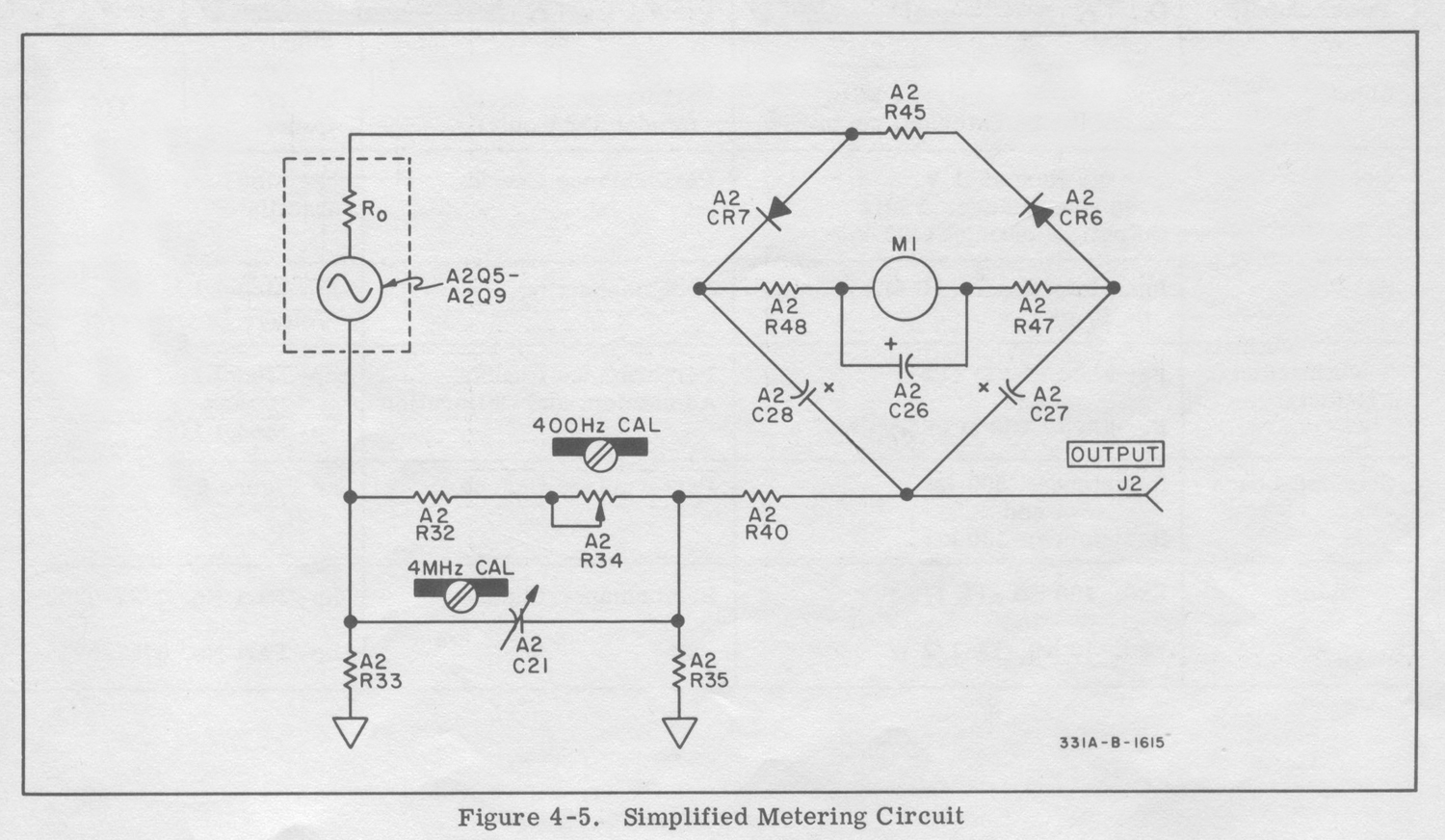
4-35. The meter rectifier is connected in abridge type of configuration with a diode in each upper arm and a dc milliammeter connected across the midpoints of the bridge. The simplified meter rectifier is illustrated in Figure 4-5. The generator represented by A2Q5 through A2Q9 , with the internal impedance R0, provides the meter M1 with current for full scale deflection and develops a voltage across the calibration network which closes the ac feedback loop. Capacitors A2C27 and A2C28 are used as coupling capacitors for the ac feedback loop and the output signal to the OUTPUT connector. The mechanical inertia of the meter prevents the meter from responding to individual current pulses; therefore the meter pointer reading corresponds to the average value of the current pulses rather than the peak value. The meter calibration is to the rms value of a sine wave. Resistor A2R45 impresses a fixed bias across diodes A2CR6 and A2CR7 (biasing them close to the barrier voltage) to make the meter circuit response linear to large variations in signal amplitude. The linearity of this type of circuit is also increased by enclosing the meter circuit in the overall feedback loop.
4-36. POWER SUPPLY CIRCUIT.
(Refer to Figure 7-4.)
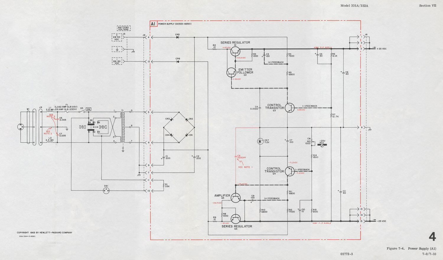
4-37. The power supply circuit consists of a +25 volt series regulated supply and a -25 volt series regulated supply which is the reference supply for the +25 volt supply.
4-38. The -25 volt regulated supply is of the conventional series regulator type. The amplifier A1Q5 is used to increase the loop gain of the circuit, thus improving voltage regulation. The positive feedback applied to the junction of A1R11 and A1R12 is used to further improve the line frequency suppression of the circuit.
4-39. The +25 volt regulated supply is of the conventional series regulator type and operates the same as the -25 volt regulated supply.
4-40. Diodes A1CR5 and A1CR6 are coupling and protection diodes for external battery supplies. The diodes protect the series regulator circuits from application of incorrect polarity at the battery input terminals. The diodes also protect external batteries from being charged in the wrong direction when the ac power is being used with batteries connected- to the battery terminals.
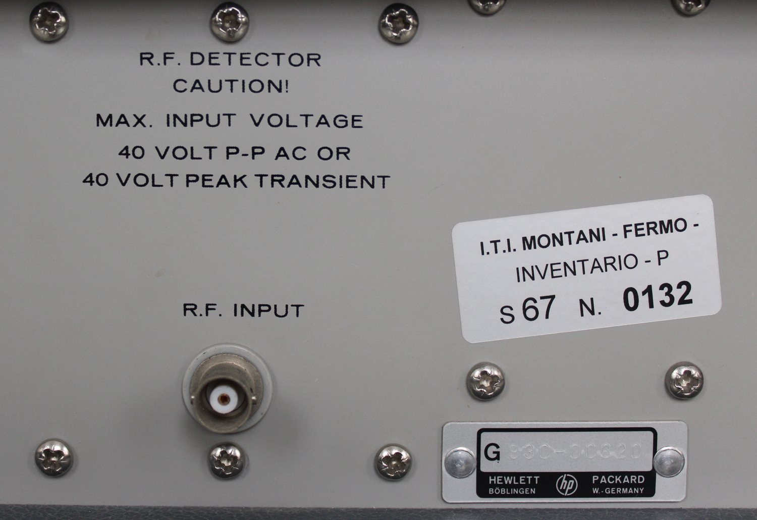
4-41. RF DETECTOR CIRCUIT (332A ONLY1.
(Refer to Figure 7-1.)
4-42. The RF detector circuit consists of a rectifier, A4CR1, and filter circuit. The RF signal is applied to the circuit through the RF INPUT connector on the rear panel. The rectifier diode A4CR1 recovers the modulating signal from the RF carrier and the filter circuit removes any RF components before the signal is applied to the impedance converter circuit through the NORM-RF DET switch S7».
§§§
Abbiamo omesso la sezione IV Maintenance.
Per consultare le altre tre parti scrivere “332A” su Cerca.
Foto di Claudio Profumieri, elaborazioni e ricerche di Fabio Panfili.
Per ingrandire le immagini cliccare su di esse col tasto destro del mouse e scegliere tra le opzioni.